-
 Agriculture
-
 Health-Care
-
 Environment
-
 Construction-Real-Estate
-
 Tools-Hardware
-
 Home-Garden
-
 Furniture
-
 Luggage-Bags-Cases
-
 Medical-devices-Supplies
-
 Gifts-Crafts
-
 Sports-Entertainment
-
 Food-Beverage
-
 Vehicles-Transportation
-
 Power-Transmission
-
 Material-Handling
-
 Renewable-Energy
-
 Safety
-
 Testing-Instrument-Equipment
-
 Construction-Building-Machinery
-
 Pet-Supplies
-
 Personal-Care-Household-Cleaning
-
 Vehicle-Accessories-Electronics-Tools
-
 School-Office-Supplies
-
 Packaging-Printing
-
 Mother-Kids-Toys
-
 Business-Services
-
 Commercial-Equipment-Machinery
-
 Apparel-Accessories
-
 Security
-
 Shoes-Accessories
-
 Vehicle-Parts-Accessories
-
 Jewelry-Eyewear-Watches-Accessories
-
 Lights-Lighting
-
 Fabric-Textile-Raw-Material
-
 Fabrication-Services
-
 Industrial-Machinery
-
 Consumer-Electronics
-
 Electrical-Equipment-Supplies
-
 Electronic-Components-Accessories-Telecommunications
-
 Home-Appliances
-
 Beauty
-
 Chemicals
-
 Rubber-Plastics
-
 Metals-Alloys
- Masonry Materials
- Curtain Walls & Accessories
- Earthwork Products
- Fireproofing Materials
- Heat Insulation Materials
- Plastic Building Materials
- Building Boards
- Soundproofing Materials
- Timber
- Waterproofing Materials
- Balustrades & Handrails
- Bathroom & Kitchen
- Flooring & Accessories
- Tiles & Accessories
- Door, Window & Accessories
- Fireplaces & Stoves
- Floor Heating Systems & Parts
- Stairs & Stair Parts
- Ceilings
- Elevators & Escalators
- Stone
- Countertops, Vanity Tops & Table Tops
- Mosaics
- Metal Building Materials
- Multifunctional Materials
- Ladders & Scaffoldings
- Mouldings
- Corner Guards
- Decorative Films
- Formwork
- Building & Industrial Glass
- Other Construction & Real Estate
- Wallpapers/Wall panels
- HVAC System & Parts
- Outdoor Facilities
- Prefabricated Buildings
- Festive & Party Supplies
- Bathroom Products
- Household Sundries
- Rain Gear
- Garden Supplies
- Household Cleaning Tools & Accessories
- Lighters & Smoking Accessories
- Home Storage & Organization
- Household Scales
- Smart Home Improvement
- Home Textiles
- Kitchenware
- Drinkware & Accessories
- Dinnerware, Coffee & Wine
- Home Decor
- Golf
- Fitness & Body Building
- Amusement Park Facilities
- Billiards, Board Game,Coin Operated Games
- Musical Instruments
- Outdoor Affordable Luxury Sports
- Camping & Hiking
- Fishing
- Sports Safety&Rehabilitation
- Ball Sports Equipments
- Water Sports
- Winter Sports
- Luxury Travel Equipments
- Sports Shoes, Bags & Accessories
- Cycling
- Other Sports & Entertainment Products
- Artificial Grass&Sports Flooring&Sports Court Equipment
- Scooters
- Food Ingredients
- Honey & Honey Products
- Snacks
- Nuts & Kernels
- Seafood
- Plant & Animal Oil
- Beverages
- Fruit & Vegetable Products
- Frog & Escargot
- Bean Products
- Egg Products
- Dairy Products
- Seasonings & Condiments
- Canned Food
- Instant Food
- Baked Goods
- Other Food & Beverage
- Meat & Poultry
- Confectionery
- Grain Products
- Feminie Care
- Hair Care & Styling
- Body Care
- Hands & Feet Care
- Hygiene Products
- Men's Grooming
- Laundry Cleaning Supplies
- Travel Size & Gift Sets
- Room Deodorizers
- Other Personal Care Products
- Pest Control Products
- Special Household Cleaning
- Floor Cleaning
- Kitchen & Bathroom Cleaning
- Oral Care
- Bath Supplies
- Yellow Pages
- Correction Supplies
- Office Binding Supplies
- Office Cutting Supplies
- Board Erasers
- Office Adhesives & Tapes
- Education Supplies
- Pencil Cases & Bags
- Notebooks & Writing Pads
- File Folder Accessories
- Calendars
- Writing Accessories
- Commercial Office Supplies
- Pencil Sharpeners
- Pens
- Letter Pad/Paper
- Paper Envelopes
- Desk Organizers
- Pencils
- Markers & Highlighters
- Filing Products
- Art Supplies
- Easels
- Badge Holder & Accessories
- Office Paper
- Printer Supplies
- Book Covers
- Other Office & School Supplies
- Stationery Set
- Boards
- Clipboards
- Stamps
- Drafting Supplies
- Stencils
- Electronic Dictionary
- Books
- Map
- Magazines
- Calculators
- Baby & Toddler Toys
- Educational Toys
- Classic Toys
- Dress Up & Pretend Play
- Toy Vehicle
- Stuffed Animals & Plush Toys
- Outdoor Toys & Structures
- Balloons & Accessories
- Baby Food
- Children's Clothing
- Baby Supplies & Products
- Maternity Clothes
- Kids Shoes
- Baby Care
- Novelty & Gag Toys
- Dolls & Accessories
- Puzzle & Games
- Blocks & Model Building Toys
- Toddler Clothing
- Baby Clothing
- Kids' Luggage & Bags
- Arts, Crafts & DIY Toys
- Action & Toy Figures
- Baby Appliances
- Hobbies & Models
- Remote Control Toys
- Promotional Toys
- Pregnancy & Maternity
- Hygiene Products
- Kid's Textile&Bedding
- Novelty & Special Use
- Toy Weapons
- Baby Gifts
- Baby Storage & Organization
- Auto Drive Systems
- ATV/UTV Parts & Accessories
- Marine Parts & Accessories
- Other Auto Parts
- Trailer Parts & Accessories
- Auto Transmission Systems
- Train Parts & Accessories
- Universal Parts
- Railway Parts & Accessories
- Auto Brake Systems
- Aviation Parts & Accessories
- Truck Parts & Accessories
- Auto Suspension Systems
- Auto Lighting Systems
- New Energy Vehicle Parts & Accessories
- Auto Steering Systems
- Wheels, Tires & Accessories
- Bus Parts & Accessories
- Auto Performance Parts
- Cooling System
- Go-Kart & Kart Racer Parts & Accessories
- Air Conditioning Systems
- Heavy Duty Vehicle Parts & Accessories
- Auto Electrical Systems
- Auto Body Systems
- Auto Engine Systems
- Container Parts & Accessories
- Motorcycle Parts & Accessories
- Refrigeration & Heat Exchange Equipment
- Machine Tool Equipment
- Food & Beverage Machinery
- Agricultural Machinery & Equipment
- Apparel & Textile Machinery
- Chemical Machinery
- Packaging Machines
- Paper Production Machinery
- Plastic & Rubber Processing Machinery
- Industrial Robots
- Electronic Products Machinery
- Metal & Metallurgy Machinery
- Woodworking Machinery
- Home Product Manufacturing Machinery
- Machinery Accessories
- Environmental Machinery
- Machinery Service
- Electrical Equipment Manufacturing Machinery
- Industrial Compressors & Parts
- Tobacco & Cigarette Machinery
- Production Line
- Used Industrial Machinery
- Electronics Production Machinery
- Other Machinery & Industrial Equipment
- Camera, Photo & Accessories
- Portable Audio, Video & Accessories
- Television, Home Audio, Video & Accessories
- Video Games & Accessories
- Mobile Phone & Accessories
- Electronic Publications
- Earphone & Headphone & Accessories
- Speakers & Accessories
- Smart Electronics
- TV Receivers & Accessories
- Mobile Phone & Computer Repair Parts
- Chargers, Batteries & Power Supplies
- Used Electronics
- VR, AR, MR Hardware & Software
- Projectors & Presentation Equipments
- Other Consumer Electronics
- Cables & Commonly Used Accessories
- Computer Hardware & Software
- Displays, Signage and Optoelectronics
- Discrete Semiconductors
- Wireless & IoT Module and Products
- Telecommunications
- Connectors, Terminals & Accessories
- Development Boards, Electronic Modules and Kits
- Circuit Protection
- Sensors
- Isolators
- Audio Components and Products
- Integrated Circuits
- Power Supplies
- Relays
- RF, Microwave and RFID
- Electronic Accessories & Supplies
- Passive Components
- PCB & PCBA
- Air Quality Appliances
- Home Appliance Parts
- Heating & Cooling Appliances
- Small Kitchen Appliances
- Laundry Appliances
- Water Heaters
- Water Treatment Appliances
- Refrigerators & Freezers
- Personal Care & Beauty Appliances
- Major Kitchen Appliances
- Cleaning Appliances
- Second-hand Appliances
- Smart Home Appliances
- Other Home Appliances
- Energy Chemicals
- Inorganic Chemicals
- Basic Organic Chemicals
- Agrochemicals
- Admixture & Additives
- Catalysts & Chemical Auxiliary Agents
- Pigments & Dyestuff
- Coating & Paint
- Daily Chemicals
- Polymer
- Organic Intermediate
- Adhesives & Sealants
- Chemical Waste
- Biological Chemical Products
- Surface Treatment Chemicals
- Painting & Coating
- Chemical Reagents
- Flavor & Fragrance
- Non-Explosive Demolition Agents
- Other Chemicals
- Custom Chemical Services
Electrical Supplies
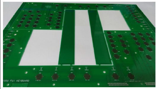
Step by Step Guide to Designing Reliable Electronic Circuits on PCBs
Designing reliable electronic circuits on printed circuit boards (PCBs) is a critical skill for engineers and hobbyists alike. Whether you're developing a simple gadget or a complex industrial system, the quality of your PCB design can make or break the final product. This step-by-step guide will walk you through the essential stages of creating robust and dependable circuits, from initial planning to final testing. By following these best practices, you can minimize errors, improve performance, and ensure longevity in your electronic designs.
Understanding the Requirements
Before diving into the design process, it's crucial to clearly define the requirements of your circuit. Start by identifying the purpose of the PCB, the components it will host, and the environmental conditions it will face. For instance, a circuit designed for a consumer device will have different constraints than one intended for aerospace applications.
Next, consider the electrical specifications, such as voltage levels, current requirements, and signal frequencies. These parameters will influence your choice of components and layout strategies. Additionally, think about thermal management, as overheating can lead to premature failure. By thoroughly understanding these requirements upfront, you can avoid costly redesigns later in the process.
Schematic Design and Component Selection
The schematic is the blueprint of your PCB, representing the electrical connections between components. Begin by selecting the right components based on your requirements. Opt for reputable manufacturers and ensure that the parts are readily available. Using off-the-shelf components can save time and reduce costs.
When drawing the schematic, pay attention to signal flow and grouping related components together. This will simplify the layout phase. Label all components clearly and include notes for any special considerations, such as high-voltage sections or sensitive analog signals. A well-organized schematic not only aids in troubleshooting but also serves as a valuable reference for future revisions.
PCB Layout and Routing
Once the schematic is finalized, the next step is translating it into a physical layout. Start by placing components strategically to minimize trace lengths and avoid interference. Group related components together and position high-frequency or noise-sensitive parts away from potential sources of interference, such as power supplies.
Routing involves connecting the components with copper traces. Use wider traces for high-current paths to reduce resistance and prevent overheating. For sensitive signals, consider differential pairs or controlled impedance routing. Always adhere to the manufacturer's design rules, such as minimum trace widths and clearances, to ensure manufacturability.
Grounding and Power Distribution
A solid grounding scheme is vital for reducing noise and ensuring signal integrity. Use a ground plane to provide a low-impedance return path for currents. Avoid splitting the ground plane unnecessarily, as this can create ground loops and introduce noise. For mixed-signal designs, separate analog and digital grounds and connect them at a single point.
Power distribution is equally important. Use decoupling capacitors near power pins to filter out high-frequency noise. Place them as close as possible to the components they serve. Additionally, consider using multiple power planes for different voltage levels to minimize cross-talk and voltage drops.
Design Verification and Testing
Before sending your design for fabrication, perform a design rule check (DRC) to catch any errors, such as short circuits or missing connections. Many PCB design tools include DRC features that can automate this process. Additionally, run a signal integrity analysis if your design involves high-speed signals.
Once the PCB is fabricated, conduct thorough testing. Start with a visual inspection to check for obvious defects. Then, use a multimeter or oscilloscope to verify voltages and signals. Functional testing should follow, where you validate the circuit's performance under real-world conditions. Document any issues and iterate on the design as needed.
Final Thoughts
Designing reliable electronic circuits on PCBs is a meticulous process that requires attention to detail at every stage. By understanding the requirements, creating a clear schematic, optimizing the layout, and rigorously testing the final product, you can achieve robust and dependable designs. Remember, the key to success lies in planning, precision, and continuous improvement.

Overcoming Common Challenges in Electronic Circuit Design for PCBs
Electronic circuit design for printed circuit boards (PCBs) is a complex and intricate process that requires a deep understanding of electrical engineering principles, material science, and manufacturing techniques. Despite advancements in technology, designers often face numerous challenges that can impact the performance, reliability, and manufacturability of their circuits. Overcoming these challenges is crucial for creating efficient, high-quality PCBs that meet the demands of modern electronics. This article explores some of the most common hurdles in PCB design and provides practical solutions to address them.
Signal Integrity and Noise Reduction
One of the most prevalent challenges in PCB design is maintaining signal integrity and minimizing noise. High-speed signals are particularly susceptible to interference, which can lead to data corruption or signal degradation. To mitigate this, designers must carefully consider trace routing, impedance matching, and grounding techniques.
Proper trace routing involves avoiding sharp angles and ensuring consistent trace widths to minimize reflections. Impedance matching is essential for high-frequency signals, as mismatches can cause signal reflections and power loss. Additionally, a well-designed grounding scheme, such as a star or ground plane, can significantly reduce noise and improve signal integrity.
Thermal Management
Heat dissipation is another critical challenge in PCB design, especially for circuits with high-power components. Excessive heat can lead to component failure, reduced lifespan, and performance degradation. Effective thermal management strategies are essential to ensure reliable operation.
Designers can use thermal vias to transfer heat away from critical components to the PCB's outer layers or heat sinks. Proper component placement is also vital; high-power components should be spaced apart to prevent localized heating. Additionally, selecting materials with high thermal conductivity, such as metal-core PCBs, can enhance heat dissipation.
Component Placement and Routing
Optimizing component placement and routing is a delicate balancing act that affects both performance and manufacturability. Poor placement can lead to signal interference, increased parasitic capacitance, and difficulties during assembly.
Designers should prioritize placing critical components, such as microcontrollers and oscillators, first to minimize signal path lengths. Grouping related components together can reduce noise and simplify routing. Automated routing tools can help, but manual adjustments are often necessary to avoid bottlenecks and ensure optimal performance.
Power Distribution and Decoupling
A stable power supply is fundamental to PCB performance, yet power distribution networks (PDNs) often pose significant challenges. Voltage drops, noise, and transient responses can disrupt circuit operation if not properly addressed.
To ensure a robust PDN, designers should use wide traces or power planes to minimize resistance and inductance. Decoupling capacitors placed close to power pins can filter high-frequency noise and stabilize voltage levels. Additionally, simulating the PDN during the design phase can help identify potential issues before fabrication.
Manufacturing Constraints and Design for Assembly (DFA)
PCB design must account for manufacturing constraints to ensure cost-effective and reliable production. Design for Assembly (DFA) principles help streamline the manufacturing process and reduce errors.
Common DFA considerations include adhering to minimum trace widths and spacing, avoiding overly complex via structures, and ensuring proper solder mask and silkscreen alignment. Collaboration with manufacturers early in the design process can help identify potential issues and optimize the design for production.
Testing and Debugging
Even with meticulous design, PCBs often require testing and debugging to identify and resolve issues. Inadequate testing can lead to costly rework or field failures.
Incorporating test points and boundary scan capabilities can facilitate debugging and validation. Prototyping and iterative testing are also crucial for catching design flaws early. Advanced simulation tools can predict potential problems, but real-world testing remains indispensable for ensuring reliability.
By addressing these common challenges, designers can create PCBs that are not only functional but also robust, manufacturable, and reliable. The key lies in a thorough understanding of the principles involved, careful planning, and iterative testing to refine the design.

Innovative Approaches to Multilayer PCB Design in Electronic Circuits
In the rapidly evolving world of electronics, the design of multilayer printed circuit boards (PCBs) has become a cornerstone of innovation. As devices grow more complex and compact, traditional PCB design methods often fall short of meeting the demands for higher performance, reduced size, and enhanced functionality. This article explores cutting-edge approaches to multilayer PCB design that are revolutionizing electronic circuits, offering engineers and designers new tools to overcome challenges and push the boundaries of what's possible.
Multilayer PCBs, which consist of multiple layers of conductive material separated by insulating layers, are essential for modern electronics. They enable higher circuit density, improved signal integrity, and better thermal management compared to single or double-layer boards. However, designing these intricate systems requires innovative techniques to address issues such as signal interference, power distribution, and manufacturing constraints. By delving into the latest advancements, this article aims to provide valuable insights into how these challenges can be tackled effectively.
Advanced Material Selection for Enhanced Performance
One of the most critical aspects of multilayer PCB design is the choice of materials. Traditional materials like FR-4 have served the industry well, but emerging technologies demand substrates with superior electrical and thermal properties. High-frequency laminates, such as Rogers or Teflon-based materials, are now being used to minimize signal loss and improve impedance control. These materials are particularly beneficial for high-speed digital and RF applications, where signal integrity is paramount.
Additionally, the use of flexible and rigid-flex materials has opened new possibilities for multilayer PCB design. Flexible PCBs can bend and fold, making them ideal for wearable devices and compact electronics. By combining rigid and flexible layers, designers can create boards that are both durable and adaptable, reducing the need for connectors and interconnects, which can introduce signal degradation. This hybrid approach not only enhances reliability but also simplifies assembly processes.
Innovative Routing Techniques for Signal Integrity
Signal integrity is a major concern in multilayer PCB design, especially as clock speeds and data rates continue to rise. To address this, designers are adopting innovative routing techniques such as differential pair routing and controlled impedance routing. Differential pairs help reduce electromagnetic interference (EMI) by ensuring that signals travel in opposite phases, canceling out noise. This technique is particularly useful for high-speed data transmission lines, such as those found in USB and HDMI interfaces.
Another groundbreaking approach is the use of via-in-pad and microvia technologies. Vias are essential for connecting different layers of a PCB, but traditional through-hole vias can introduce parasitic capacitance and inductance. Via-in-pad places vias directly under component pads, reducing the distance signals must travel and minimizing parasitic effects. Microvias, which are smaller and drilled with lasers, further enhance density and performance by allowing for finer pitch connections and reducing signal path lengths.
Thermal Management Strategies
As electronic devices become more powerful, managing heat dissipation in multilayer PCBs has become a critical challenge. Excessive heat can degrade performance and shorten the lifespan of components. To combat this, designers are incorporating advanced thermal management strategies, such as embedded heat sinks and thermal vias. Embedded heat sinks are integrated directly into the PCB layers, providing efficient heat dissipation without adding bulk. Thermal vias, on the other hand, are strategically placed to conduct heat away from hot spots and distribute it evenly across the board.
Another innovative approach is the use of thermally conductive materials, such as metal-core PCBs or ceramic substrates. These materials offer superior heat dissipation compared to traditional FR-4, making them ideal for high-power applications like LED lighting and power electronics. By combining these materials with intelligent layout designs, engineers can ensure that heat is managed effectively, maintaining optimal performance and reliability.
Design for Manufacturability (DFM) and Automation
Designing a multilayer PCB is only half the battle; ensuring that it can be manufactured efficiently and cost-effectively is equally important. Design for Manufacturability (DFM) principles are now being integrated into the design process to minimize errors and reduce production costs. This includes adhering to manufacturer-specific guidelines, optimizing panel layouts, and avoiding overly complex designs that could lead to yield issues.
Automation is also playing a pivotal role in multilayer PCB design. Advanced software tools, such as AI-driven design assistants and automated routing algorithms, are helping designers streamline their workflows and identify potential issues early in the process. These tools can analyze vast amounts of data to suggest optimal component placements, routing paths, and layer stackups, significantly reducing design time and improving overall quality. By leveraging automation, designers can focus on innovation rather than tedious manual tasks.
Future Trends and Emerging Technologies
The future of multilayer PCB design is brimming with exciting possibilities. One promising trend is the integration of additive manufacturing, or 3D printing, into PCB production. This technology allows for the creation of complex, multi-material structures that were previously impossible to achieve with traditional methods. For example, 3D-printed PCBs could incorporate conductive traces, insulating layers, and even embedded components in a single manufacturing step, revolutionizing the way circuits are built.
Another emerging technology is the use of embedded active and passive components. By embedding components within the PCB layers, designers can further reduce board size and improve performance. This approach eliminates the need for surface-mounted components, reducing parasitic effects and enhancing signal integrity. As these technologies mature, they are expected to become standard practices in multilayer PCB design, enabling even greater innovation in electronic circuits.
In conclusion, the field of multilayer PCB design is undergoing a transformation driven by innovative materials, advanced routing techniques, thermal management strategies, and automation. These approaches are not only addressing current challenges but also paving the way for future advancements. As electronics continue to evolve, designers who embrace these cutting-edge techniques will be well-positioned to create the next generation of high-performance, reliable, and compact devices.

Exploring Advanced Techniques in Electronic Circuit Design for PCB Layout
Electronic circuit design for PCB (Printed Circuit Board) layout is a critical aspect of modern electronics, influencing the performance, reliability, and efficiency of devices. As technology advances, the demand for more compact, high-speed, and energy-efficient circuits has grown exponentially. This article, Exploring Advanced Techniques in Electronic Circuit Design for PCB Layout, delves into the cutting-edge methodologies that engineers and designers employ to overcome the challenges of contemporary PCB design. Whether you're a seasoned professional or an aspiring engineer, understanding these techniques will equip you with the knowledge to create innovative and robust electronic systems.
The evolution of PCB design has been remarkable, transitioning from simple single-layer boards to complex multi-layer architectures with high-density interconnects. Today, designers must navigate challenges such as signal integrity, thermal management, and electromagnetic interference (EMI) while adhering to stringent size and power constraints. This article explores advanced techniques that address these challenges, offering insights into optimizing performance and ensuring reliability in PCB layouts.
Signal Integrity and High-Speed Design
Signal integrity is paramount in high-speed PCB design, where even minor distortions can lead to significant performance degradation. Advanced techniques such as impedance matching, controlled impedance routing, and differential signaling are employed to maintain signal quality. Impedance matching ensures that the signal propagates without reflections, while controlled impedance routing maintains consistent impedance across traces, reducing signal distortion.
Differential signaling, another critical technique, involves transmitting signals over paired traces with opposite polarity. This method enhances noise immunity and reduces EMI, making it ideal for high-speed data transmission. Additionally, designers use simulation tools to analyze signal behavior and identify potential issues before fabrication, saving time and resources.
Thermal Management Strategies
Effective thermal management is essential to prevent overheating and ensure the longevity of electronic components. Advanced PCB designs incorporate thermal vias, heat sinks, and thermal pads to dissipate heat efficiently. Thermal vias are small holes filled with conductive material that transfer heat from components to other layers or the PCB's exterior. Heat sinks, often made of aluminum or copper, are attached to high-power components to enhance heat dissipation.
Another innovative approach is the use of embedded cooling channels, where microfluidic channels are integrated into the PCB to circulate coolant and remove heat. This technique is particularly useful in high-power applications such as servers and automotive electronics. By optimizing thermal management, designers can improve performance and reliability while extending the lifespan of electronic devices.
EMI and EMC Considerations
Electromagnetic interference (EMI) and electromagnetic compatibility (EMC) are critical concerns in PCB design, especially in devices operating at high frequencies. Advanced techniques such as proper grounding, shielding, and careful component placement are employed to mitigate EMI. Ground planes, for instance, provide a low-impedance path for return currents, reducing noise and interference.
Shielding involves enclosing sensitive components or traces in conductive materials to block external EMI. Additionally, designers use techniques like spread spectrum clocking to reduce peak emissions and comply with EMC regulations. By addressing EMI and EMC early in the design process, engineers can ensure that their devices operate reliably in diverse environments.
Multi-Layer PCB Design
Multi-layer PCBs are increasingly common in modern electronics, offering higher component density and improved performance. Designing multi-layer boards requires careful planning of layer stack-up, signal routing, and power distribution. Advanced techniques such as blind and buried vias are used to connect specific layers without occupying unnecessary space, enabling more compact designs.
Power integrity is another critical aspect of multi-layer PCB design. Proper decoupling capacitor placement and power plane segmentation ensure stable voltage distribution and minimize noise. By leveraging these techniques, designers can create high-performance multi-layer PCBs that meet the demands of today's complex electronic systems.
Design for Manufacturability (DFM)
Design for Manufacturability (DFM) is a proactive approach that ensures PCB designs can be efficiently and cost-effectively manufactured. Advanced DFM techniques include adhering to minimum trace widths and spacing, avoiding acute angles in traces, and optimizing pad sizes for soldering. These practices reduce the risk of manufacturing defects and improve yield rates.
Collaboration between designers and manufacturers is also crucial for successful DFM. By involving manufacturers early in the design process, potential issues can be identified and resolved before production begins. This collaborative approach not only saves time and money but also enhances the overall quality of the final product.
In conclusion, exploring advanced techniques in electronic circuit design for PCB layout is essential for creating high-performance, reliable, and manufacturable electronic devices. By mastering these methodologies, designers can push the boundaries of innovation and meet the ever-evolving demands of the electronics industry.
REPORT


