-
 Agriculture
-
 Health-Care
-
 Environment
-
 Construction-Real-Estate
-
 Tools-Hardware
-
 Home-Garden
-
 Furniture
-
 Luggage-Bags-Cases
-
 Medical-devices-Supplies
-
 Gifts-Crafts
-
 Sports-Entertainment
-
 Food-Beverage
-
 Vehicles-Transportation
-
 Power-Transmission
-
 Material-Handling
-
 Renewable-Energy
-
 Safety
-
 Testing-Instrument-Equipment
-
 Construction-Building-Machinery
-
 Pet-Supplies
-
 Personal-Care-Household-Cleaning
-
 Vehicle-Accessories-Electronics-Tools
-
 School-Office-Supplies
-
 Packaging-Printing
-
 Mother-Kids-Toys
-
 Business-Services
-
 Commercial-Equipment-Machinery
-
 Apparel-Accessories
-
 Security
-
 Shoes-Accessories
-
 Vehicle-Parts-Accessories
-
 Jewelry-Eyewear-Watches-Accessories
-
 Lights-Lighting
-
 Fabric-Textile-Raw-Material
-
 Fabrication-Services
-
 Industrial-Machinery
-
 Consumer-Electronics
-
 Electrical-Equipment-Supplies
-
 Electronic-Components-Accessories-Telecommunications
-
 Home-Appliances
-
 Beauty
-
 Chemicals
-
 Rubber-Plastics
-
 Metals-Alloys
- Masonry Materials
- Curtain Walls & Accessories
- Earthwork Products
- Fireproofing Materials
- Heat Insulation Materials
- Plastic Building Materials
- Building Boards
- Soundproofing Materials
- Timber
- Waterproofing Materials
- Balustrades & Handrails
- Bathroom & Kitchen
- Flooring & Accessories
- Tiles & Accessories
- Door, Window & Accessories
- Fireplaces & Stoves
- Floor Heating Systems & Parts
- Stairs & Stair Parts
- Ceilings
- Elevators & Escalators
- Stone
- Countertops, Vanity Tops & Table Tops
- Mosaics
- Metal Building Materials
- Multifunctional Materials
- Ladders & Scaffoldings
- Mouldings
- Corner Guards
- Decorative Films
- Formwork
- Building & Industrial Glass
- Other Construction & Real Estate
- Wallpapers/Wall panels
- HVAC System & Parts
- Outdoor Facilities
- Prefabricated Buildings
- Festive & Party Supplies
- Bathroom Products
- Household Sundries
- Rain Gear
- Garden Supplies
- Household Cleaning Tools & Accessories
- Lighters & Smoking Accessories
- Home Storage & Organization
- Household Scales
- Smart Home Improvement
- Home Textiles
- Kitchenware
- Drinkware & Accessories
- Dinnerware, Coffee & Wine
- Home Decor
- Golf
- Fitness & Body Building
- Amusement Park Facilities
- Billiards, Board Game,Coin Operated Games
- Musical Instruments
- Outdoor Affordable Luxury Sports
- Camping & Hiking
- Fishing
- Sports Safety&Rehabilitation
- Ball Sports Equipments
- Water Sports
- Winter Sports
- Luxury Travel Equipments
- Sports Shoes, Bags & Accessories
- Cycling
- Other Sports & Entertainment Products
- Artificial Grass&Sports Flooring&Sports Court Equipment
- Scooters
- Food Ingredients
- Honey & Honey Products
- Snacks
- Nuts & Kernels
- Seafood
- Plant & Animal Oil
- Beverages
- Fruit & Vegetable Products
- Frog & Escargot
- Bean Products
- Egg Products
- Dairy Products
- Seasonings & Condiments
- Canned Food
- Instant Food
- Baked Goods
- Other Food & Beverage
- Meat & Poultry
- Confectionery
- Grain Products
- Feminie Care
- Hair Care & Styling
- Body Care
- Hands & Feet Care
- Hygiene Products
- Men's Grooming
- Laundry Cleaning Supplies
- Travel Size & Gift Sets
- Room Deodorizers
- Other Personal Care Products
- Pest Control Products
- Special Household Cleaning
- Floor Cleaning
- Kitchen & Bathroom Cleaning
- Oral Care
- Bath Supplies
- Yellow Pages
- Correction Supplies
- Office Binding Supplies
- Office Cutting Supplies
- Board Erasers
- Office Adhesives & Tapes
- Education Supplies
- Pencil Cases & Bags
- Notebooks & Writing Pads
- File Folder Accessories
- Calendars
- Writing Accessories
- Commercial Office Supplies
- Pencil Sharpeners
- Pens
- Letter Pad/Paper
- Paper Envelopes
- Desk Organizers
- Pencils
- Markers & Highlighters
- Filing Products
- Art Supplies
- Easels
- Badge Holder & Accessories
- Office Paper
- Printer Supplies
- Book Covers
- Other Office & School Supplies
- Stationery Set
- Boards
- Clipboards
- Stamps
- Drafting Supplies
- Stencils
- Electronic Dictionary
- Books
- Map
- Magazines
- Calculators
- Baby & Toddler Toys
- Educational Toys
- Classic Toys
- Dress Up & Pretend Play
- Toy Vehicle
- Stuffed Animals & Plush Toys
- Outdoor Toys & Structures
- Balloons & Accessories
- Baby Food
- Children's Clothing
- Baby Supplies & Products
- Maternity Clothes
- Kids Shoes
- Baby Care
- Novelty & Gag Toys
- Dolls & Accessories
- Puzzle & Games
- Blocks & Model Building Toys
- Toddler Clothing
- Baby Clothing
- Kids' Luggage & Bags
- Arts, Crafts & DIY Toys
- Action & Toy Figures
- Baby Appliances
- Hobbies & Models
- Remote Control Toys
- Promotional Toys
- Pregnancy & Maternity
- Hygiene Products
- Kid's Textile&Bedding
- Novelty & Special Use
- Toy Weapons
- Baby Gifts
- Baby Storage & Organization
- Auto Drive Systems
- ATV/UTV Parts & Accessories
- Marine Parts & Accessories
- Other Auto Parts
- Trailer Parts & Accessories
- Auto Transmission Systems
- Train Parts & Accessories
- Universal Parts
- Railway Parts & Accessories
- Auto Brake Systems
- Aviation Parts & Accessories
- Truck Parts & Accessories
- Auto Suspension Systems
- Auto Lighting Systems
- New Energy Vehicle Parts & Accessories
- Auto Steering Systems
- Wheels, Tires & Accessories
- Bus Parts & Accessories
- Auto Performance Parts
- Cooling System
- Go-Kart & Kart Racer Parts & Accessories
- Air Conditioning Systems
- Heavy Duty Vehicle Parts & Accessories
- Auto Electrical Systems
- Auto Body Systems
- Auto Engine Systems
- Container Parts & Accessories
- Motorcycle Parts & Accessories
- Refrigeration & Heat Exchange Equipment
- Machine Tool Equipment
- Food & Beverage Machinery
- Agricultural Machinery & Equipment
- Apparel & Textile Machinery
- Chemical Machinery
- Packaging Machines
- Paper Production Machinery
- Plastic & Rubber Processing Machinery
- Industrial Robots
- Electronic Products Machinery
- Metal & Metallurgy Machinery
- Woodworking Machinery
- Home Product Manufacturing Machinery
- Machinery Accessories
- Environmental Machinery
- Machinery Service
- Electrical Equipment Manufacturing Machinery
- Industrial Compressors & Parts
- Tobacco & Cigarette Machinery
- Production Line
- Used Industrial Machinery
- Electronics Production Machinery
- Other Machinery & Industrial Equipment
- Camera, Photo & Accessories
- Portable Audio, Video & Accessories
- Television, Home Audio, Video & Accessories
- Video Games & Accessories
- Mobile Phone & Accessories
- Electronic Publications
- Earphone & Headphone & Accessories
- Speakers & Accessories
- Smart Electronics
- TV Receivers & Accessories
- Mobile Phone & Computer Repair Parts
- Chargers, Batteries & Power Supplies
- Used Electronics
- VR, AR, MR Hardware & Software
- Projectors & Presentation Equipments
- Other Consumer Electronics
- Cables & Commonly Used Accessories
- Computer Hardware & Software
- Displays, Signage and Optoelectronics
- Discrete Semiconductors
- Wireless & IoT Module and Products
- Telecommunications
- Connectors, Terminals & Accessories
- Development Boards, Electronic Modules and Kits
- Circuit Protection
- Sensors
- Isolators
- Audio Components and Products
- Integrated Circuits
- Power Supplies
- Relays
- RF, Microwave and RFID
- Electronic Accessories & Supplies
- Passive Components
- PCB & PCBA
- Air Quality Appliances
- Home Appliance Parts
- Heating & Cooling Appliances
- Small Kitchen Appliances
- Laundry Appliances
- Water Heaters
- Water Treatment Appliances
- Refrigerators & Freezers
- Personal Care & Beauty Appliances
- Major Kitchen Appliances
- Cleaning Appliances
- Second-hand Appliances
- Smart Home Appliances
- Other Home Appliances
- Energy Chemicals
- Inorganic Chemicals
- Basic Organic Chemicals
- Agrochemicals
- Admixture & Additives
- Catalysts & Chemical Auxiliary Agents
- Pigments & Dyestuff
- Coating & Paint
- Daily Chemicals
- Polymer
- Organic Intermediate
- Adhesives & Sealants
- Chemical Waste
- Biological Chemical Products
- Surface Treatment Chemicals
- Painting & Coating
- Chemical Reagents
- Flavor & Fragrance
- Non-Explosive Demolition Agents
- Other Chemicals
- Custom Chemical Services
PCB & PCBA
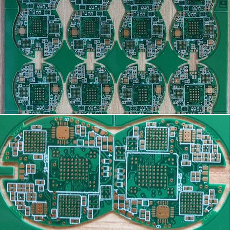
Implementing Design For Manufacturing Guidelines In PCB Layout Projects
In the intricate world of electronics development, the journey from a schematic diagram to a functional, mass-produced printed circuit board (PCB) is fraught with potential pitfalls. While a PCB layout might appear flawless in simulation, its real-world manufacturability ultimately determines project success, cost, and time-to-market. This is where the systematic application of Design for Manufacturing (DFM) guidelines becomes paramount. Implementing DFM in PCB layout projects is not merely a final checklist but a foundational philosophy integrated throughout the design process. It serves as the critical bridge between the theoretical design and the practical realities of fabrication and assembly, ensuring that brilliant ideas are translated into reliable, high-yield, and cost-effective physical products. By proactively addressing manufacturing constraints during layout, engineers can avoid costly re-spins, delays, and quality issues, making DFM an indispensable discipline in modern electronics design.
Fundamental DFM Principles in Component Placement and Footprint Design
The initial stages of PCB layout, particularly component placement and footprint creation, set the stage for manufacturability. Adherence to DFM begins with the library. Each component footprint must be meticulously designed according to the manufacturer's datasheet, ensuring accurate pad sizes, shapes, and spacing. Pads that are too small can lead to poor solder joints, while oversized pads may cause bridging or tombstoning during reflow soldering. Furthermore, incorporating clear silkscreen outlines and polarity markers within the footprint aids assembly technicians and reduces placement errors.
Strategic component placement is equally crucial. A core DFM tenet is orienting similar components in the same direction, typically 0° or 90°, to optimize the pick-and-place machine's movement and speed. Sufficient spacing must be maintained between components to allow for the solder paste stencil aperture, the soldering iron tip for potential rework, and automated optical inspection (AOI) equipment. Special attention is required for large, heavy components like connectors or heatsinks, which may need additional mechanical support or specific placement to prevent warping during soldering or stress during use. By mastering these placement rules, designers create a layout that is not only electrically sound but also optimized for automated assembly lines.
Optimizing Trace Routing and Copper Features for Fabrication Yield
Once components are placed, the routing of traces and definition of copper pours must conform to the capabilities of the PCB fabricator. This involves adhering to a set of minimum design rules dictated by the chosen manufacturer's process. Key parameters include minimum trace width and spacing, which directly impact the board's current-carrying capacity, impedance control, and susceptibility to short circuits. Pushing these limits to the absolute minimum increases cost and reduces fabrication yield; therefore, using wider traces and greater clearances where possible enhances reliability.
Copper balancing is another critical, yet often overlooked, DFM consideration. Large areas of copper on one layer without corresponding copper on opposite layers can cause the board to warp during the high-temperature lamination process. This warpage can lead to registration issues in multilayer boards and problems during assembly. To mitigate this, designers should use hatched copper pours or add thieving—non-connected copper shapes—on sparse layers. Additionally, avoiding acute angles in traces and ensuring adequate annular rings for vias and through-hole pads prevent acid traps during etching and weak mechanical connections, respectively. These practices ensure the bare board is robust and consistently producible.
Incorporating Assembly and Testability Features from the Start
DFM extends beyond fabrication to encompass the entire assembly and test process. A layout must be designed for efficient and error-free population with components. This involves providing adequate clearance around the board edges for handling by conveyor belts in assembly machines and including tooling holes or fiducial markers. Global and local fiducials—precise copper markers—are essential for vision systems on pick-and-place machines to accurately align the board and place components, especially for fine-pitch BGAs or QFNs.
Design for Testability (DFT), a subset of DFM, is integral to ensuring product quality. This means incorporating test points for critical nets to allow for in-circuit testing (ICT) or flying probe testing. These test points must be accessible, properly sized, and located away from tall components. For boards requiring boundary-scan testing, adhering to JTAG chain requirements during layout is vital. Furthermore, considering rework accessibility by avoiding placing large components directly over vias or sensitive areas can save significant time and cost during debugging and repair phases. By designing with assembly and test in mind, the transition from populated board to verified product becomes seamless and efficient.
Leveraging DFM Analysis Tools and Collaboration with Partners
Successfully implementing DFM guidelines is greatly facilitated by modern electronic design automation (EDA) tools. Most advanced PCB layout software includes built-in DFM rule checks that can validate designs against user-defined or manufacturer-supplied rule sets. These automated checks can flag issues like silkscreen over pads, insufficient solder mask slivers, or copper too close to the board edge, which might be tedious to find manually. Running these checks iteratively throughout the design process, rather than just at the end, allows for early correction of potential faults.
However, tools are only as good as the rules they use. The most effective DFM strategy involves early and ongoing collaboration with manufacturing partners. Engaging with your chosen PCB fabricator and assembly house during the design phase allows you to tailor your layout to their specific equipment, processes, and capabilities. They can provide their most up-to-date process capability matrices, recommending optimal values for hole sizes, copper weights, and solder mask expansion. This collaborative approach transforms DFM from a generic set of rules into a targeted, optimized practice, dramatically increasing the likelihood of first-pass success and building a stronger, more predictable supply chain.

Designing Robust Power Distribution Networks In Complex Electronics Layouts
In the intricate world of modern electronics, where devices are shrinking in size yet exploding in functionality, lies a critical and often underappreciated challenge: ensuring clean, stable power reaches every transistor. The design of a Power Distribution Network (PDN) is the unsung hero of electronic systems, acting as the circulatory system that delivers lifeblood—electrical energy—to all active components. In complex layouts featuring high-speed processors, dense memory arrays, and mixed-signal blocks, a poorly designed PDN can lead to catastrophic failures, subtle performance degradation, or intermittent bugs that are notoriously difficult to diagnose. As clock speeds soar and supply voltages plummet to save power, the margin for error vanishes. This article delves into the art and science of designing robust Power Distribution Networks, exploring the fundamental principles and advanced strategies necessary to achieve resilience in the face of escalating complexity.
The Critical Role of Impedance and Decoupling
At the heart of a robust PDN lies the imperative to maintain a low impedance across a broad frequency spectrum, from DC to gigahertz. The target impedance, calculated from the allowable voltage ripple and the dynamic current draw of the load, serves as the primary design goal. A network with high impedance at certain frequencies acts as a bottleneck, causing significant voltage droop or ground bounce when components switch states, potentially leading to logic errors or timing violations.
Achieving this low impedance is a multi-tiered endeavor, heavily reliant on strategic decoupling. Bulk capacitors, with high capacitance values, handle low-frequency current demands and stabilize the DC voltage. Mid-frequency decoupling is typically managed by ceramic capacitors placed on the board. However, the most critical challenge arises at high frequencies, where the parasitic inductance of capacitor leads and board traces dominates. Here, the solution involves placing small, low-inductance capacitors (like multilayer ceramic chip capacitors) extremely close to the power pins of integrated circuits. Furthermore, the effective use of power and ground plane pairs in the PCB itself creates inherent, low-inductance distributed capacitance, which is essential for suppressing very high-frequency noise.
Navigating Complexity in Physical Layout
The physical implementation of the PDN in a dense, multi-layer PCB is where theory meets reality. A fundamental strategy is the use of dedicated, solid power and ground planes. These planes provide a low-inductance current return path, which is as crucial as the delivery path itself for controlling noise and electromagnetic interference (EMI). Splitting planes for multiple voltage domains must be done with extreme care to avoid creating accidental antennas or forcing return currents to take long, inductive detours.
Another critical layout consideration is the management of via transitions. Vias connecting components to internal planes introduce inductance and resistance. For high-current paths, such as those supplying a microprocessor core, designers must use multiple vias in parallel to reduce this parasitic impedance. The placement of decoupling capacitors is a spatial puzzle; they must be positioned to minimize the loop area formed by the capacitor, its via connections to the power and ground planes, and the IC it serves. In the most demanding applications, this leads to the use of embedded capacitance within the PCB substrate or integrated passive devices (IPDs) placed directly within the IC package.
Analysis, Simulation, and Verification
Designing a PDN for a complex system is not a task left to intuition. It requires rigorous analysis and simulation throughout the design cycle. Before layout begins, system-level simulations model the current profiles of major ICs to estimate worst-case transient demands. Tools for frequency-domain analysis, such as impedance (Z-parameter) plots, are indispensable for verifying that the network meets the target impedance across frequency.
Once a layout is drafted, electromagnetic (EM) field solvers are used to extract the parasitic resistance, inductance, and capacitance (RLC) of the actual copper shapes, planes, and vias. This extracted model is then simulated in the time domain with realistic current stimuli to check for voltage transients. The final stage of verification often involves measurement on prototype boards using vector network analyzers (VNAs) to measure impedance and oscilloscopes with high-bandwidth differential probes to capture voltage ripple, ensuring the simulated performance aligns with physical reality.
Addressing Advanced Challenges: Noise and Integrity
Beyond basic delivery, a robust PDN must safeguard signal integrity and system stability. A primary threat is simultaneous switching noise (SSN), where many output drivers switch at once, causing a collective surge in current demand that can collapse the local supply voltage. Mitigation involves providing ample local decoupling, using dedicated power/ground pairs for I/O banks, and implementing staggered switching times in silicon if possible.
In mixed-signal systems, the PDN design becomes even more delicate. Analog circuits, such as data converters or radio frequency (RF) blocks, are highly sensitive to digital noise coupling through the shared power supply. Techniques like using separate, quiet linear regulators for analog supplies, implementing "moats" or splits in the ground plane with careful bridging at a single point, and employing ferrite beads or isolation filters are common strategies to preserve analog purity. Ultimately, designing a robust PDN is a holistic exercise in balancing electrical performance, physical constraints, and cost to create a foundation upon which complex electronics can reliably and efficiently operate.

Efficient Thermal Management Strategies For Dense Electronics Layout Design
In the relentless pursuit of miniaturization and enhanced performance, modern electronic systems are being packed with an ever-increasing number of components into shrinking form factors. This trend towards dense electronics layout design, while enabling powerful and compact devices, brings forth a critical and often formidable challenge: thermal management. Excessive heat is the nemesis of electronic reliability, leading to accelerated component degradation, timing errors, reduced efficiency, and ultimately, system failure. Efficient thermal management is no longer a secondary consideration but a fundamental pillar of successful electronics design, directly impacting product longevity, safety, and performance. This article delves into the core strategies essential for mastering heat dissipation in densely packed electronic assemblies, exploring a multi-faceted approach from the silicon level to the system enclosure.
Component-Level Optimization and Strategic Placement
The foundation of effective thermal management begins at the most granular level: the components themselves and their arrangement on the printed circuit board (PCB). Designers must prioritize the selection of components with lower thermal resistance and higher power efficiency where possible. Furthermore, the physical layout is paramount. High-power components, such as processors, power regulators, and FPGAs, should not be clustered together, as this creates concentrated hotspots that are extremely difficult to cool.
Strategic placement involves distributing these heat-generating devices across the board to allow for more uniform heat spreading. Utilizing thermal vias—plated through-holes that conduct heat from the component's thermal pad into the inner ground planes or to the opposite side of the board—is a critical technique. These vias act as efficient vertical conduits, transferring heat away from the surface-mounted device into the board's bulk copper layers, which then act as a heat spreader. Careful attention must also be paid to the orientation of components to ensure they do not obstruct the natural airflow paths that might be established within the system.
Advanced PCB Design and Material Selection
The PCB itself can be engineered to be an active participant in thermal management. Beyond standard FR-4 material, designers can opt for substrates with higher thermal conductivity, such as metal-core PCBs (MCPCBs) or ceramics. In an MCPCB, a layer of dielectric material is bonded to a metal baseplate (typically aluminum), providing an excellent path for heat to travel from components to the board's edge or to an attached heatsink.
Another sophisticated approach involves the use of embedded copper structures or inlays. These are solid blocks of copper embedded within the PCB stack-up directly beneath high-power components. They offer significantly lower thermal resistance than a field of thermal vias, effectively pulling heat laterally through the board. Additionally, maximizing the use of internal copper planes—especially ground planes—and connecting them thermally to hot components helps to spread heat over a larger area, reducing the thermal gradient and making secondary cooling methods more effective.
Integrated Cooling Solutions: Heatsinks and Heat Pipes
For components generating substantial heat, passive cooling in the form of attached heatsinks is indispensable. In dense layouts, the design of the heatsink becomes crucial. Finned heatsinks increase the surface area for convective heat transfer, but their size and orientation must be carefully planned to fit within spatial constraints and align with airflow. For severely limited spaces, custom-shaped heatsinks or even integrating finned structures into the device's enclosure itself can be effective solutions.
When direct conduction to a chassis or external heatsink is not feasible, heat pipes offer a remarkably efficient means of transporting heat over distance. A heat pipe is a sealed tube containing a wick structure and a small amount of working fluid. It operates on a continuous cycle of evaporation and condensation, moving heat from a hot spot (the evaporator section attached to the component) to a cooler area (the condenser section attached to a larger heatsink or chassis wall) with minimal temperature difference. This allows designers to relocate the primary heat dissipation point away from congested areas on the board.
System-Level Airflow Management and Active Cooling
The overall system architecture must facilitate the removal of heat from the board and the enclosure. This involves meticulous airflow management. Designers should aim to create a defined, low-resistance path for air to travel, typically using a combination of strategically placed intake and exhaust vents. The layout should guide air directly over the hottest components and their associated heatsinks, avoiding dead zones where stagnant air can lead to heat buildup.
When passive and conductive methods are insufficient, active cooling with fans or blowers becomes necessary. The selection between axial fans (for higher airflow at lower pressure) and blowers (for higher pressure to force air through dense, restricted pathways) is critical. In dense designs, blowers are often more effective. Implementing intelligent fan control, where fan speed is dynamically adjusted based on real-time temperature sensors, optimizes cooling performance while minimizing acoustic noise and power consumption. Computational Fluid Dynamics (CFD) simulations are an invaluable tool during the design phase to model and optimize airflow patterns before physical prototyping.
Emerging Technologies and Holistic Design Philosophy
The frontier of thermal management continues to advance with innovative solutions. Liquid cooling, once confined to high-performance computing, is becoming more accessible for compact systems through cold plates or micro-channel coolers that interface directly with high-power chips. Phase-change materials (PCMs), which absorb large amounts of heat as they melt, are being explored for managing transient thermal spikes. Additionally, advanced thermal interface materials (TIMs), such as graphene-based pads or liquid metal compounds, are improving the crucial thermal connection between components and heatsinks.
Ultimately, the most efficient thermal management strategy arises from a holistic, co-design philosophy. Thermal considerations must be integrated from the very inception of the product design, running in parallel with electrical and mechanical design cycles. This proactive approach, leveraging simulation, careful material choice, and a hierarchy of cooling methods from component to system level, is the key to unlocking the full potential of dense electronics layout design without succumbing to the pitfalls of overheating.

Advanced Electronics Layout Design For High Speed Circuit Board Applications
In the rapidly evolving landscape of modern electronics, the demand for higher data rates, greater bandwidth, and enhanced performance has pushed circuit design into the realm of high-speed signals. This is where the specialized discipline of "Advanced Electronics Layout Design for High-Speed Circuit Board Applications" becomes not just relevant, but absolutely critical. It moves far beyond the basic connectivity of traditional PCB layout, entering a domain where every trace, via, and component placement is a calculated decision to preserve signal integrity, manage electromagnetic interference, and ensure reliable operation at gigahertz frequencies. From cutting-edge telecommunications infrastructure and high-performance computing servers to advanced automotive radar and medical imaging systems, the principles of advanced high-speed layout are the invisible backbone enabling technological breakthroughs. This article delves into the core aspects of this sophisticated field, exploring the fundamental challenges and methodologies that define successful high-speed PCB implementation.
Signal Integrity: The Paramount Consideration
At the heart of high-speed design lies the imperative of maintaining signal integrity (SI). As signal edge rates become incredibly fast—often in the picosecond range—traces on the board no longer behave as simple wires but as transmission lines. When the electrical length of a trace approaches a significant fraction of the signal's wavelength, effects like reflection, crosstalk, and attenuation dominate. A primary tool for controlling these effects is impedance matching. Designers must meticulously calculate and control the characteristic impedance of traces (commonly 50 or 100 ohms for differential pairs) through precise management of trace width, dielectric material thickness, and copper weight. A mismatch in impedance causes signal reflections, leading to overshoot, undershoot, and data errors at the receiver.
Furthermore, managing signal paths for critical nets, such as clocks and high-speed data buses, requires strict length matching and topology control. Designers employ techniques like serpentine routing to add deliberate delay, ensuring that related signals arrive simultaneously at their destination. The choice of routing strategy—whether point-to-point, daisy-chain, or fly-by—is dictated by the specific protocol (e.g., DDR memory, PCI Express). Neglecting these SI principles results in a board that may power on but will fail under operational conditions, with intermittent glitches and corrupted data that are notoriously difficult to diagnose.
Power Integrity and Advanced Power Distribution Network (PDN) Design
A stable and clean power supply is the foundation upon which signal integrity is built. In high-speed circuits, the Power Distribution Network (PDN) is a dynamic, frequency-dependent system. The primary challenge is to provide a low-impedance path for current from the power source to every integrated circuit across a broad frequency range, from DC up to several gigahertz. Transient switching currents from modern processors and FPGAs can be massive and rapid, causing voltage droops or ground bounce if the PDN is inadequate. This directly impacts noise margins and can cause false switching.
To achieve this, advanced layout employs a multi-layered strategy. This includes the use of dedicated power and ground planes in a multilayer stack-up to provide inherent capacitance and low inductance. Strategic placement of decoupling capacitors is crucial: bulk capacitors handle lower frequency demands, while a hierarchy of smaller, low-inductance ceramic capacitors are placed as close as possible to device power pins to suppress high-frequency noise. The design of the PDN is often supported by sophisticated simulation tools that model the impedance profile (Z11) to identify resonant frequencies and ensure the impedance stays below the target threshold across the required bandwidth.
Electromagnetic Compatibility (EMC) and Controlled Impedance Routing
High-speed designs must not only function internally but also comply with stringent electromagnetic compatibility (EMC) regulations, limiting both emissions and susceptibility. A poorly laid-out high-speed board can act as an efficient antenna, radiating noise and causing interference with other devices, or failing immunity tests. Controlled impedance routing, as mentioned for SI, is equally vital for EMC. Properly terminated transmission lines minimize ringing and reduce high-frequency harmonic content that leads to radiation.
Layout techniques to enhance EMC include providing uninterrupted ground planes as return paths for high-speed currents, minimizing loop areas by routing signal traces close to their reference plane, and using guard traces or ground shielding for extremely sensitive nets. The placement and filtering of I/O connectors where high-speed signals enter or exit the board are critical zones. Furthermore, the stack-up design itself is a powerful EMC tool. Symmetrical, tightly coupled layer arrangements with buried signal layers between ground planes can effectively contain electromagnetic fields, turning the PCB into a shielded enclosure for its signals.
Material Selection and Stack-up Architecture
The physical construction of the PCB, defined by its materials and layer stack-up, is a fundamental design choice made before a single component is placed. For high-speed applications, standard FR-4 material may not suffice at higher frequencies due to its more lossy nature and less stable dielectric constant (Dk). Advanced laminates with lower dissipation factor (Df) and tightly controlled Dk, such as Rogers, Isola, or specialized Megtron grades, are often employed for critical high-frequency layers to reduce signal attenuation and phase distortion.
The stack-up architecture determines the electrical environment for every trace. A well-planned stack-up assigns dedicated layers for power and ground, ensuring short return paths and defining controlled impedance. It also considers the proximity of signal layers to their reference planes and the order of layers to manage crosstalk between adjacent signal layers. Decisions on copper weight, dielectric thickness, and prepreg material all feed into the impedance calculations and overall thermal and mechanical performance of the assembly. This pre-layout planning phase is arguably one of the most important steps in guaranteeing a successful high-speed design.
Utilization of Advanced Design and Analysis Tools
The complexity of modern high-speed layouts makes reliance on experience and manual calculation insufficient. The field is now driven by a suite of powerful electronic design automation (EDA) tools. These tools integrate schematic capture, layout, and, most importantly, pre-layout and post-layout simulation. SI/PI analysis tools can extract parasitic parameters from the physical layout, simulate eye diagrams to predict data integrity, and analyze power plane resonances.
3D electromagnetic field solvers are used to model complex structures like connectors, vias, and antennas. Furthermore, design rule checking (DRC) has evolved into constraint-driven design, where electrical rules (e.g., length, delay, impedance) are defined upfront and the layout tool actively guides the designer to comply. This iterative process of design, simulate, analyze, and refine is essential for first-pass success, reducing costly board spins and development time in projects where performance margins are razor-thin.
REPORT

