-
 Agriculture
-
 Health-Care
-
 Environment
-
 Construction-Real-Estate
-
 Tools-Hardware
-
 Home-Garden
-
 Furniture
-
 Luggage-Bags-Cases
-
 Medical-devices-Supplies
-
 Gifts-Crafts
-
 Sports-Entertainment
-
 Food-Beverage
-
 Vehicles-Transportation
-
 Power-Transmission
-
 Material-Handling
-
 Renewable-Energy
-
 Safety
-
 Testing-Instrument-Equipment
-
 Construction-Building-Machinery
-
 Pet-Supplies
-
 Personal-Care-Household-Cleaning
-
 Vehicle-Accessories-Electronics-Tools
-
 School-Office-Supplies
-
 Packaging-Printing
-
 Mother-Kids-Toys
-
 Business-Services
-
 Commercial-Equipment-Machinery
-
 Apparel-Accessories
-
 Security
-
 Shoes-Accessories
-
 Vehicle-Parts-Accessories
-
 Jewelry-Eyewear-Watches-Accessories
-
 Lights-Lighting
-
 Fabric-Textile-Raw-Material
-
 Fabrication-Services
-
 Industrial-Machinery
-
 Consumer-Electronics
-
 Electrical-Equipment-Supplies
-
 Electronic-Components-Accessories-Telecommunications
-
 Home-Appliances
-
 Beauty
-
 Chemicals
-
 Rubber-Plastics
-
 Metals-Alloys
- Masonry Materials
- Curtain Walls & Accessories
- Earthwork Products
- Fireproofing Materials
- Heat Insulation Materials
- Plastic Building Materials
- Building Boards
- Soundproofing Materials
- Timber
- Waterproofing Materials
- Balustrades & Handrails
- Bathroom & Kitchen
- Flooring & Accessories
- Tiles & Accessories
- Door, Window & Accessories
- Fireplaces & Stoves
- Floor Heating Systems & Parts
- Stairs & Stair Parts
- Ceilings
- Elevators & Escalators
- Stone
- Countertops, Vanity Tops & Table Tops
- Mosaics
- Metal Building Materials
- Multifunctional Materials
- Ladders & Scaffoldings
- Mouldings
- Corner Guards
- Decorative Films
- Formwork
- Building & Industrial Glass
- Other Construction & Real Estate
- Wallpapers/Wall panels
- HVAC System & Parts
- Outdoor Facilities
- Prefabricated Buildings
- Festive & Party Supplies
- Bathroom Products
- Household Sundries
- Rain Gear
- Garden Supplies
- Household Cleaning Tools & Accessories
- Lighters & Smoking Accessories
- Home Storage & Organization
- Household Scales
- Smart Home Improvement
- Home Textiles
- Kitchenware
- Drinkware & Accessories
- Dinnerware, Coffee & Wine
- Home Decor
- Golf
- Fitness & Body Building
- Amusement Park Facilities
- Billiards, Board Game,Coin Operated Games
- Musical Instruments
- Outdoor Affordable Luxury Sports
- Camping & Hiking
- Fishing
- Sports Safety&Rehabilitation
- Ball Sports Equipments
- Water Sports
- Winter Sports
- Luxury Travel Equipments
- Sports Shoes, Bags & Accessories
- Cycling
- Other Sports & Entertainment Products
- Artificial Grass&Sports Flooring&Sports Court Equipment
- Scooters
- Food Ingredients
- Honey & Honey Products
- Snacks
- Nuts & Kernels
- Seafood
- Plant & Animal Oil
- Beverages
- Fruit & Vegetable Products
- Frog & Escargot
- Bean Products
- Egg Products
- Dairy Products
- Seasonings & Condiments
- Canned Food
- Instant Food
- Baked Goods
- Other Food & Beverage
- Meat & Poultry
- Confectionery
- Grain Products
- Feminie Care
- Hair Care & Styling
- Body Care
- Hands & Feet Care
- Hygiene Products
- Men's Grooming
- Laundry Cleaning Supplies
- Travel Size & Gift Sets
- Room Deodorizers
- Other Personal Care Products
- Pest Control Products
- Special Household Cleaning
- Floor Cleaning
- Kitchen & Bathroom Cleaning
- Oral Care
- Bath Supplies
- Yellow Pages
- Correction Supplies
- Office Binding Supplies
- Office Cutting Supplies
- Board Erasers
- Office Adhesives & Tapes
- Education Supplies
- Pencil Cases & Bags
- Notebooks & Writing Pads
- File Folder Accessories
- Calendars
- Writing Accessories
- Commercial Office Supplies
- Pencil Sharpeners
- Pens
- Letter Pad/Paper
- Paper Envelopes
- Desk Organizers
- Pencils
- Markers & Highlighters
- Filing Products
- Art Supplies
- Easels
- Badge Holder & Accessories
- Office Paper
- Printer Supplies
- Book Covers
- Other Office & School Supplies
- Stationery Set
- Boards
- Clipboards
- Stamps
- Drafting Supplies
- Stencils
- Electronic Dictionary
- Books
- Map
- Magazines
- Calculators
- Baby & Toddler Toys
- Educational Toys
- Classic Toys
- Dress Up & Pretend Play
- Toy Vehicle
- Stuffed Animals & Plush Toys
- Outdoor Toys & Structures
- Balloons & Accessories
- Baby Food
- Children's Clothing
- Baby Supplies & Products
- Maternity Clothes
- Kids Shoes
- Baby Care
- Novelty & Gag Toys
- Dolls & Accessories
- Puzzle & Games
- Blocks & Model Building Toys
- Toddler Clothing
- Baby Clothing
- Kids' Luggage & Bags
- Arts, Crafts & DIY Toys
- Action & Toy Figures
- Baby Appliances
- Hobbies & Models
- Remote Control Toys
- Promotional Toys
- Pregnancy & Maternity
- Hygiene Products
- Kid's Textile&Bedding
- Novelty & Special Use
- Toy Weapons
- Baby Gifts
- Baby Storage & Organization
- Auto Drive Systems
- ATV/UTV Parts & Accessories
- Marine Parts & Accessories
- Other Auto Parts
- Trailer Parts & Accessories
- Auto Transmission Systems
- Train Parts & Accessories
- Universal Parts
- Railway Parts & Accessories
- Auto Brake Systems
- Aviation Parts & Accessories
- Truck Parts & Accessories
- Auto Suspension Systems
- Auto Lighting Systems
- New Energy Vehicle Parts & Accessories
- Auto Steering Systems
- Wheels, Tires & Accessories
- Bus Parts & Accessories
- Auto Performance Parts
- Cooling System
- Go-Kart & Kart Racer Parts & Accessories
- Air Conditioning Systems
- Heavy Duty Vehicle Parts & Accessories
- Auto Electrical Systems
- Auto Body Systems
- Auto Engine Systems
- Container Parts & Accessories
- Motorcycle Parts & Accessories
- Refrigeration & Heat Exchange Equipment
- Machine Tool Equipment
- Food & Beverage Machinery
- Agricultural Machinery & Equipment
- Apparel & Textile Machinery
- Chemical Machinery
- Packaging Machines
- Paper Production Machinery
- Plastic & Rubber Processing Machinery
- Industrial Robots
- Electronic Products Machinery
- Metal & Metallurgy Machinery
- Woodworking Machinery
- Home Product Manufacturing Machinery
- Machinery Accessories
- Environmental Machinery
- Machinery Service
- Electrical Equipment Manufacturing Machinery
- Industrial Compressors & Parts
- Tobacco & Cigarette Machinery
- Production Line
- Used Industrial Machinery
- Electronics Production Machinery
- Other Machinery & Industrial Equipment
- Camera, Photo & Accessories
- Portable Audio, Video & Accessories
- Television, Home Audio, Video & Accessories
- Video Games & Accessories
- Mobile Phone & Accessories
- Electronic Publications
- Earphone & Headphone & Accessories
- Speakers & Accessories
- Smart Electronics
- TV Receivers & Accessories
- Mobile Phone & Computer Repair Parts
- Chargers, Batteries & Power Supplies
- Used Electronics
- VR, AR, MR Hardware & Software
- Projectors & Presentation Equipments
- Other Consumer Electronics
- Cables & Commonly Used Accessories
- Computer Hardware & Software
- Displays, Signage and Optoelectronics
- Discrete Semiconductors
- Wireless & IoT Module and Products
- Telecommunications
- Connectors, Terminals & Accessories
- Development Boards, Electronic Modules and Kits
- Circuit Protection
- Sensors
- Isolators
- Audio Components and Products
- Integrated Circuits
- Power Supplies
- Relays
- RF, Microwave and RFID
- Electronic Accessories & Supplies
- Passive Components
- PCB & PCBA
- Air Quality Appliances
- Home Appliance Parts
- Heating & Cooling Appliances
- Small Kitchen Appliances
- Laundry Appliances
- Water Heaters
- Water Treatment Appliances
- Refrigerators & Freezers
- Personal Care & Beauty Appliances
- Major Kitchen Appliances
- Cleaning Appliances
- Second-hand Appliances
- Smart Home Appliances
- Other Home Appliances
- Energy Chemicals
- Inorganic Chemicals
- Basic Organic Chemicals
- Agrochemicals
- Admixture & Additives
- Catalysts & Chemical Auxiliary Agents
- Pigments & Dyestuff
- Coating & Paint
- Daily Chemicals
- Polymer
- Organic Intermediate
- Adhesives & Sealants
- Chemical Waste
- Biological Chemical Products
- Surface Treatment Chemicals
- Painting & Coating
- Chemical Reagents
- Flavor & Fragrance
- Non-Explosive Demolition Agents
- Other Chemicals
- Custom Chemical Services
Other Consumer Electronics
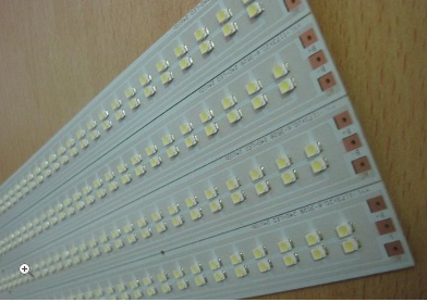
Advanced LED PCB Assembly Techniques Used
Surface Mount Technology (SMT) and Miniaturization
Surface Mount Technology (SMT) is the cornerstone of modern LED PCB assembly. Unlike through-hole technology, SMT places components directly onto the surface of the PCB, enabling significant miniaturization. This is particularly crucial for LED applications where space is often limited, such as in smartphones, smartwatches, and automotive headlamps. SMT also allows for higher component density, leading to smaller and more compact designs.
Further advancements in SMT involve the use of smaller, finer-pitch components. This requires highly precise placement equipment and advanced soldering techniques to ensure reliable connections. The use of automated pick-and-place machines, capable of placing components with sub-millimeter accuracy, is vital in mass production environments.
Advanced Soldering Techniques
The reliability of LED PCB assemblies hinges heavily on the quality of the solder joints. Traditional wave soldering is often insufficient for the intricate designs and delicate components found in modern LED applications. Instead, reflow soldering, a process that melts solder paste to create connections, is widely used. This technique offers greater precision and control, minimizing the risk of damage to sensitive components.
Beyond standard reflow, advanced techniques like laser soldering and selective soldering are gaining traction. Laser soldering offers highly localized heating, enabling the precise soldering of individual components without affecting neighboring parts. Selective soldering allows for the targeted application of solder paste, reducing material waste and improving overall efficiency.
High-Density Interconnects (HDI)
As the complexity of LED applications increases, so does the need for higher component density and more intricate circuit designs. High-Density Interconnects (HDI) PCBs address this by incorporating multiple layers and finer trace widths, allowing for a greater number of components and connections within a smaller space. This is crucial for applications requiring high brightness and complex light patterns.
Manufacturing HDI PCBs requires sophisticated techniques, including buried vias and blind vias, which allow for connections between internal layers without penetrating the top or bottom surfaces. These advanced techniques contribute to increased miniaturization and improved signal integrity.
Automated Optical Inspection (AOI) and X-Ray Inspection
Ensuring the quality and reliability of LED PCB assemblies requires rigorous testing and inspection. Automated Optical Inspection (AOI) systems use cameras and sophisticated algorithms to detect defects in solder joints, component placement, and other critical aspects of the assembly process. This automated approach significantly enhances efficiency and accuracy compared to manual inspection.
For more intricate inspections, particularly those involving hidden solder joints or internal defects, X-ray inspection is employed. This non-destructive testing method allows for the visualization of internal components and connections, ensuring the structural integrity of the assembly. This is especially critical for complex multi-layer PCBs.
Material Selection and Thermal Management
The performance and lifespan of LEDs are significantly impacted by thermal management. Advanced LED PCB assembly techniques incorporate materials with high thermal conductivity to dissipate heat effectively. This can involve using specialized substrates, heat sinks, and thermal vias to ensure optimal operating temperatures and prevent premature failure of the LEDs.
Careful selection of materials is also crucial for other aspects of the assembly. The PCB material itself, the solder paste composition, and even the encapsulant used to protect the LEDs all impact the overall reliability and performance of the final product. Choosing appropriate materials is therefore a crucial aspect of advanced LED PCB assembly.

CuttingEdge Flexible Edge Plating Technology
Enhanced Flexibility and Durability
Unlike traditional plating methods that often lead to brittle connections, Cutting-Edge Flexible Edge Plating Technology utilizes advanced materials and processes to ensure superior flexibility and durability. The plating process itself is carefully optimized to minimize stress concentration points, preventing cracking or delamination during bending or flexing. This enhanced flexibility is crucial for applications requiring repeated bending and folding, such as wearable devices, foldable phones, and flexible displays.
Furthermore, the choice of plating materials plays a significant role in the overall durability. The technology often employs specialized alloys and coatings that exhibit excellent corrosion resistance, ensuring long-term reliability even in harsh environments. This enhanced durability reduces the likelihood of connection failures, contributing to the overall longevity and dependability of the electronic device.
Precise and Uniform Plating
Achieving consistent and precise plating is paramount for reliable electronic connections. Cutting-Edge Flexible Edge Plating Technology leverages advanced automation and precise control systems to ensure highly uniform plating thickness across the entire edge connector. This meticulous control minimizes variations in electrical conductivity and ensures optimal signal integrity. Any inconsistencies in plating can lead to hotspots, increased resistance, and ultimately, system failures.
The technology employs sophisticated monitoring and feedback mechanisms to guarantee the desired plating thickness and uniformity. This precise control allows for the creation of intricate edge connectors with complex geometries, catering to the demanding requirements of modern electronic devices. The precision also facilitates the integration of smaller and denser components, contributing to miniaturization efforts.
Miniaturization and High-Density Interconnects
The ability to create highly miniaturized and high-density interconnects is a key advantage of Cutting-Edge Flexible Edge Plating Technology. The process enables the creation of incredibly fine features and tight tolerances, allowing for increased component density on a smaller footprint. This is particularly advantageous for wearable electronics and other space-constrained applications where minimizing size and weight is paramount.
This miniaturization capability directly contributes to improved performance and reduced power consumption. Smaller components lead to shorter signal paths, resulting in faster data transmission speeds and lower signal attenuation. The resulting higher density interconnects allow for the integration of more complex circuitry within the same physical space, expanding functionality without compromising size.
Cost-Effectiveness and Scalability
While the technology may initially seem complex, Cutting-Edge Flexible Edge Plating Technology is designed with cost-effectiveness and scalability in mind. The automated processes involved significantly reduce labor costs and improve manufacturing throughput. This allows for large-scale production, making the technology suitable for mass-market applications.
The optimized processes and reduced waste inherent in the technology contribute to its overall cost-competitiveness. Furthermore, the improved yield and reduced rework associated with consistent and reliable plating translate to significant savings in the long run. This makes the technology an attractive option for manufacturers seeking to balance innovation with economic viability.
Applications and Future Trends
The applications for Cutting-Edge Flexible Edge Plating Technology are vast and diverse. From flexible displays and wearable electronics to medical implants and automotive applications, this technology is poised to revolutionize the way electronic devices are designed and manufactured. The ability to create robust and highly flexible connections opens up exciting possibilities for next-generation devices with enhanced functionality and user experiences.
Future trends suggest further advancements in materials science and process optimization, pushing the boundaries of miniaturization and performance. Research is ongoing to explore new plating materials with even greater flexibility, conductivity, and durability. The integration of advanced sensing and actuation capabilities directly into flexible circuits is also anticipated, leading to even more sophisticated and innovative applications.

Precise Flexible Edge Plating Board Systems
Enhanced Flexibility and Design Freedom
The core advantage of Precise Flexible Edge Plating Board Systems lies in their inherent flexibility. Unlike traditional rigid PCBs, these systems utilize flexible substrates, typically polyimide films, allowing for intricate folding, bending, and conformal shaping. This opens up a world of possibilities for designers, enabling them to create compact, space-saving designs that can conform to irregular surfaces. This is particularly crucial in applications where space is at a premium, such as wearable electronics, implantable medical devices, and automotive electronics. The flexibility also enables the creation of complex 3D assemblies, significantly reducing the need for multiple rigid boards and simplifying the overall system architecture.
This flexibility extends beyond just the physical form factor. The design process itself benefits from the increased freedom offered by these systems. Engineers can more readily incorporate components into tight spaces and optimize routing for signal integrity and EMI/RFI shielding. The ability to route traces around obstacles without the constraints imposed by rigid substrates allows for more efficient use of board space and a streamlined design process. This translates to reduced design cycles and faster time-to-market for new products.
Superior Thermal Management
High-performance electronics generate significant heat, and efficient thermal management is crucial for reliable operation and preventing system failure. Precise Flexible Edge Plating Board Systems address this challenge effectively through several mechanisms. The flexible substrate itself can be designed to incorporate heat-dissipating materials, enhancing heat transfer away from critical components. This can be further enhanced by integrating heat sinks or using advanced thermal interface materials directly onto the flexible substrate. The ability to conform to irregular surfaces allows for better contact with heat sinks and other cooling solutions, improving thermal performance significantly.
Furthermore, the flexibility allows for innovative thermal management strategies. For example, heat-generating components can be strategically positioned to maximize convective cooling or positioned closer to cooling channels. This targeted approach, combined with the material properties of the flexible substrate, creates a highly efficient thermal management system that extends the operational lifespan and reliability of the electronics.
High-Density Interconnects
Precise Flexible Edge Plating Board Systems support high-density interconnects, enabling the integration of a greater number of components within a smaller footprint. This is achieved through advanced micro-via technology and fine-line trace capabilities, which allow for smaller component spacing and complex routing patterns. This translates to increased functionality and performance within a smaller form factor. The flexibility of the substrate further enhances this capability, allowing for tighter bends and more efficient use of space compared to traditional rigid PCBs.
The precision of the edge plating process ensures reliable connections and consistent electrical performance. This precision is critical for high-speed signals, where signal integrity is paramount. The consistent quality of the plating ensures minimal signal loss and impedance matching, leading to improved system performance and reliability. This makes these systems ideal for high-speed data transmission applications.
Manufacturing and Assembly Considerations
While offering significant advantages, the manufacturing and assembly of Precise Flexible Edge Plating Board Systems require specialized techniques and equipment. The flexible nature of the substrate necessitates careful handling and precise alignment during the manufacturing process. However, advancements in automated assembly and handling systems are mitigating these challenges. Specialized pick-and-place machines, along with advancements in soldering and adhesive bonding techniques, are enabling efficient and reliable manufacturing processes.
The flexibility also presents unique challenges for testing and inspection. Advanced inspection methods, such as automated optical inspection (AOI) and X-ray inspection, are increasingly being used to ensure the quality and reliability of these systems. These techniques are crucial for identifying any defects or inconsistencies in the complex circuitry and ensuring the overall integrity of the finished product.
In conclusion, Precise Flexible Edge Plating Board Systems offer a compelling solution for a wide range of applications demanding high density, flexibility, and superior thermal management. While manufacturing considerations exist, the advantages offered in terms of design freedom, performance enhancement, and miniaturization are driving their increasing adoption across various industries. As technology continues to advance, these systems will likely play an even more significant role in shaping the future of electronic packaging.
NextGen Flexible Edge Plating Board Control
Enhanced Precision and Accuracy
The core advantage of NextGen Flexible Edge Plating Board Control lies in its unparalleled precision. Traditional methods often rely on fixed parameters and lack the ability to adapt to variations in board geometry or material properties. This can lead to inconsistencies in plating thickness, resulting in weak connections or even outright failures. NextGen employs advanced sensor technology and sophisticated algorithms to monitor the plating process in real-time. These sensors continuously measure crucial parameters, such as current density, plating thickness, and solution temperature, allowing for immediate adjustments to maintain consistent quality across the entire board. This dynamic control ensures that even the most intricate edge geometries receive uniform plating, minimizing the risk of defects and maximizing the reliability of the final product.
Furthermore, the system’s sophisticated algorithms allow for precise control of the plating process parameters, optimizing them based on the specific requirements of each board. This means that manufacturers can achieve the desired plating thickness with exceptional accuracy, eliminating the need for over-plating (which can lead to increased costs and potential for cracking) or under-plating (which compromises the integrity of the connection). This precision not only improves the quality of the final product but also reduces waste, contributing to a more sustainable and cost-effective manufacturing process.
Increased Flexibility and Adaptability
NextGen's flexibility is a key differentiator. It's designed to handle a wide range of board sizes, geometries, and materials, unlike many conventional systems that are limited to specific types of PCBs. This versatility significantly reduces the need for specialized tooling and fixtures, leading to cost savings and shorter setup times. The system’s adaptability extends to the types of plating solutions it can handle, allowing manufacturers to choose the optimal solution for their specific application, further enhancing the flexibility and efficiency of the entire process.
This adaptability is crucial in today's rapidly evolving electronics industry, where new designs and materials are constantly emerging. NextGen's flexible architecture enables easy integration with existing manufacturing lines and readily accommodates new technologies and processes. This future-proofing aspect ensures that manufacturers remain competitive and capable of adapting to the changing demands of the market without substantial capital investment in new equipment.
Improved Process Efficiency and Reduced Costs
Beyond precision and flexibility, NextGen leads to significant improvements in process efficiency. The real-time monitoring and control features minimize the occurrence of defects, reducing the need for rework and scrap. This translates to a considerable reduction in production costs and lead times. By optimizing the plating process, the system also contributes to reduced material consumption and waste generation, aligning with the growing emphasis on sustainable manufacturing practices.
The overall reduction in downtime resulting from fewer defects and quicker setup times further contributes to improved efficiency. This translates directly to cost savings, as manufacturers can produce more boards in less time with less waste. The intuitive user interface and automated features also minimize the need for highly skilled operators, streamlining labor costs and making the system accessible to a wider range of manufacturers.
Enhanced Data Analysis and Process Optimization
NextGen incorporates advanced data analytics capabilities, providing manufacturers with valuable insights into their plating process. The system collects real-time data on various parameters, creating a comprehensive database that can be used for process optimization and continuous improvement. This data allows manufacturers to identify trends, pinpoint potential problems, and make informed decisions to enhance efficiency and quality.
The data collected can be used to optimize plating parameters, reducing waste and improving yield. This continuous improvement loop allows manufacturers to fine-tune their processes over time, leading to further cost reductions and enhanced product quality. The ability to track performance trends also enables proactive maintenance, preventing potential downtime and ensuring consistent operational reliability.
In conclusion, NextGen Flexible Edge Plating Board Control represents a paradigm shift in PCB manufacturing. Its superior precision, flexibility, efficiency, and data-driven optimization capabilities address the challenges of modern electronics production, enabling manufacturers to produce high-quality PCBs more efficiently and cost-effectively. The technology's adaptability ensures its relevance in a dynamic industry, making it a crucial investment for manufacturers seeking a competitive edge in the years to come.REPORT

