-
 Agriculture
-
 Health-Care
-
 Environment
-
 Construction-Real-Estate
-
 Tools-Hardware
-
 Home-Garden
-
 Furniture
-
 Luggage-Bags-Cases
-
 Medical-devices-Supplies
-
 Gifts-Crafts
-
 Sports-Entertainment
-
 Food-Beverage
-
 Vehicles-Transportation
-
 Power-Transmission
-
 Material-Handling
-
 Renewable-Energy
-
 Safety
-
 Testing-Instrument-Equipment
-
 Construction-Building-Machinery
-
 Pet-Supplies
-
 Personal-Care-Household-Cleaning
-
 Vehicle-Accessories-Electronics-Tools
-
 School-Office-Supplies
-
 Packaging-Printing
-
 Mother-Kids-Toys
-
 Business-Services
-
 Commercial-Equipment-Machinery
-
 Apparel-Accessories
-
 Security
-
 Shoes-Accessories
-
 Vehicle-Parts-Accessories
-
 Jewelry-Eyewear-Watches-Accessories
-
 Lights-Lighting
-
 Fabric-Textile-Raw-Material
-
 Fabrication-Services
-
 Industrial-Machinery
-
 Consumer-Electronics
-
 Electrical-Equipment-Supplies
-
 Electronic-Components-Accessories-Telecommunications
-
 Home-Appliances
-
 Beauty
-
 Chemicals
-
 Rubber-Plastics
-
 Metals-Alloys


")


- Masonry Materials
- Curtain Walls & Accessories
- Earthwork Products
- Fireproofing Materials
- Heat Insulation Materials
- Plastic Building Materials
- Building Boards
- Soundproofing Materials
- Timber
- Waterproofing Materials
- Balustrades & Handrails
- Bathroom & Kitchen
- Flooring & Accessories
- Tiles & Accessories
- Door, Window & Accessories
- Fireplaces & Stoves
- Floor Heating Systems & Parts
- Stairs & Stair Parts
- Ceilings
- Elevators & Escalators
- Stone
- Countertops, Vanity Tops & Table Tops
- Mosaics
- Metal Building Materials
- Multifunctional Materials
- Ladders & Scaffoldings
- Mouldings
- Corner Guards
- Decorative Films
- Formwork
- Building & Industrial Glass
- Other Construction & Real Estate
- Wallpapers/Wall panels
- HVAC System & Parts
- Outdoor Facilities
- Prefabricated Buildings
- Festive & Party Supplies
- Bathroom Products
- Household Sundries
- Rain Gear
- Garden Supplies
- Household Cleaning Tools & Accessories
- Lighters & Smoking Accessories
- Home Storage & Organization
- Household Scales
- Smart Home Improvement
- Home Textiles
- Kitchenware
- Drinkware & Accessories
- Dinnerware, Coffee & Wine
- Home Decor
- Golf
- Fitness & Body Building
- Amusement Park Facilities
- Billiards, Board Game,Coin Operated Games
- Musical Instruments
- Outdoor Affordable Luxury Sports
- Camping & Hiking
- Fishing
- Sports Safety&Rehabilitation
- Ball Sports Equipments
- Water Sports
- Winter Sports
- Luxury Travel Equipments
- Sports Shoes, Bags & Accessories
- Cycling
- Other Sports & Entertainment Products
- Artificial Grass&Sports Flooring&Sports Court Equipment
- Scooters
- Food Ingredients
- Honey & Honey Products
- Snacks
- Nuts & Kernels
- Seafood
- Plant & Animal Oil
- Beverages
- Fruit & Vegetable Products
- Frog & Escargot
- Bean Products
- Egg Products
- Dairy Products
- Seasonings & Condiments
- Canned Food
- Instant Food
- Baked Goods
- Other Food & Beverage
- Meat & Poultry
- Confectionery
- Grain Products
- Feminie Care
- Hair Care & Styling
- Body Care
- Hands & Feet Care
- Hygiene Products
- Men's Grooming
- Laundry Cleaning Supplies
- Travel Size & Gift Sets
- Room Deodorizers
- Other Personal Care Products
- Pest Control Products
- Special Household Cleaning
- Floor Cleaning
- Kitchen & Bathroom Cleaning
- Oral Care
- Bath Supplies
- Yellow Pages
- Correction Supplies
- Office Binding Supplies
- Office Cutting Supplies
- Board Erasers
- Office Adhesives & Tapes
- Education Supplies
- Pencil Cases & Bags
- Notebooks & Writing Pads
- File Folder Accessories
- Calendars
- Writing Accessories
- Commercial Office Supplies
- Pencil Sharpeners
- Pens
- Letter Pad/Paper
- Paper Envelopes
- Desk Organizers
- Pencils
- Markers & Highlighters
- Filing Products
- Art Supplies
- Easels
- Badge Holder & Accessories
- Office Paper
- Printer Supplies
- Book Covers
- Other Office & School Supplies
- Stationery Set
- Boards
- Clipboards
- Stamps
- Drafting Supplies
- Stencils
- Electronic Dictionary
- Books
- Map
- Magazines
- Calculators
- Baby & Toddler Toys
- Educational Toys
- Classic Toys
- Dress Up & Pretend Play
- Toy Vehicle
- Stuffed Animals & Plush Toys
- Outdoor Toys & Structures
- Balloons & Accessories
- Baby Food
- Children's Clothing
- Baby Supplies & Products
- Maternity Clothes
- Kids Shoes
- Baby Care
- Novelty & Gag Toys
- Dolls & Accessories
- Puzzle & Games
- Blocks & Model Building Toys
- Toddler Clothing
- Baby Clothing
- Kids' Luggage & Bags
- Arts, Crafts & DIY Toys
- Action & Toy Figures
- Baby Appliances
- Hobbies & Models
- Remote Control Toys
- Promotional Toys
- Pregnancy & Maternity
- Hygiene Products
- Kid's Textile&Bedding
- Novelty & Special Use
- Toy Weapons
- Baby Gifts
- Baby Storage & Organization
- Auto Drive Systems
- ATV/UTV Parts & Accessories
- Marine Parts & Accessories
- Other Auto Parts
- Trailer Parts & Accessories
- Auto Transmission Systems
- Train Parts & Accessories
- Universal Parts
- Railway Parts & Accessories
- Auto Brake Systems
- Aviation Parts & Accessories
- Truck Parts & Accessories
- Auto Suspension Systems
- Auto Lighting Systems
- New Energy Vehicle Parts & Accessories
- Auto Steering Systems
- Wheels, Tires & Accessories
- Bus Parts & Accessories
- Auto Performance Parts
- Cooling System
- Go-Kart & Kart Racer Parts & Accessories
- Air Conditioning Systems
- Heavy Duty Vehicle Parts & Accessories
- Auto Electrical Systems
- Auto Body Systems
- Auto Engine Systems
- Container Parts & Accessories
- Motorcycle Parts & Accessories
- Refrigeration & Heat Exchange Equipment
- Machine Tool Equipment
- Food & Beverage Machinery
- Agricultural Machinery & Equipment
- Apparel & Textile Machinery
- Chemical Machinery
- Packaging Machines
- Paper Production Machinery
- Plastic & Rubber Processing Machinery
- Industrial Robots
- Electronic Products Machinery
- Metal & Metallurgy Machinery
- Woodworking Machinery
- Home Product Manufacturing Machinery
- Machinery Accessories
- Environmental Machinery
- Machinery Service
- Electrical Equipment Manufacturing Machinery
- Industrial Compressors & Parts
- Tobacco & Cigarette Machinery
- Production Line
- Used Industrial Machinery
- Electronics Production Machinery
- Other Machinery & Industrial Equipment
- Camera, Photo & Accessories
- Portable Audio, Video & Accessories
- Television, Home Audio, Video & Accessories
- Video Games & Accessories
- Mobile Phone & Accessories
- Electronic Publications
- Earphone & Headphone & Accessories
- Speakers & Accessories
- Smart Electronics
- TV Receivers & Accessories
- Mobile Phone & Computer Repair Parts
- Chargers, Batteries & Power Supplies
- Used Electronics
- VR, AR, MR Hardware & Software
- Projectors & Presentation Equipments
- Other Consumer Electronics
- Cables & Commonly Used Accessories
- Computer Hardware & Software
- Displays, Signage and Optoelectronics
- Discrete Semiconductors
- Wireless & IoT Module and Products
- Telecommunications
- Connectors, Terminals & Accessories
- Development Boards, Electronic Modules and Kits
- Circuit Protection
- Sensors
- Isolators
- Audio Components and Products
- Integrated Circuits
- Power Supplies
- Relays
- RF, Microwave and RFID
- Electronic Accessories & Supplies
- Passive Components
- PCB & PCBA
- Air Quality Appliances
- Home Appliance Parts
- Heating & Cooling Appliances
- Small Kitchen Appliances
- Laundry Appliances
- Water Heaters
- Water Treatment Appliances
- Refrigerators & Freezers
- Personal Care & Beauty Appliances
- Major Kitchen Appliances
- Cleaning Appliances
- Second-hand Appliances
- Smart Home Appliances
- Other Home Appliances
- Energy Chemicals
- Inorganic Chemicals
- Basic Organic Chemicals
- Agrochemicals
- Admixture & Additives
- Catalysts & Chemical Auxiliary Agents
- Pigments & Dyestuff
- Coating & Paint
- Daily Chemicals
- Polymer
- Organic Intermediate
- Adhesives & Sealants
- Chemical Waste
- Biological Chemical Products
- Surface Treatment Chemicals
- Painting & Coating
- Chemical Reagents
- Flavor & Fragrance
- Non-Explosive Demolition Agents
- Other Chemicals
- Custom Chemical Services

Featured Blogs

Material Selection and Characterization
The foundation of advanced impedance control lies in careful material selection. Dielectric materials play a crucial role in determining the impedance of the PCB. Manufacturers must select materials with precise dielectric constants and low dissipation factors to maintain impedance consistency. This often involves rigorous testing and characterization of materials to ensure they meet the specified tolerances. Advanced techniques, such as time-domain reflectometry (TDR), are employed to measure the dielectric properties of the materials with high accuracy.
Furthermore, the metallization layers, typically copper, must possess consistent thickness and surface roughness. Variations in these parameters directly affect the characteristic impedance. Precise control over plating processes is crucial, often involving techniques like electroless plating and electroplating with stringent monitoring to ensure uniformity across the entire board.
Design for Impedance Control
Effective impedance control begins with the PCB design stage. Computer-aided design (CAD) software plays a pivotal role in simulating and predicting impedance characteristics. Engineers utilize specialized software packages to model the signal paths, considering the dielectric properties of the materials and the geometry of the traces. This allows for optimization of trace width, spacing, and layer stacking to achieve the desired impedance.
Controlled impedance design incorporates specific trace geometries and spacing to ensure consistent impedance across the entire signal path. This may involve using microstrip, stripline, or embedded coplanar waveguide structures, each with its own impedance characteristics. Careful consideration is given to the via placement and design to minimize impedance discontinuities. These design optimizations are critical for maintaining signal integrity in high-speed applications.
Manufacturing Processes and Quality Control
The manufacturing process itself is crucial for realizing the designed impedance. Precise control over the etching and drilling processes is essential to maintain the fidelity of the trace geometry. Advanced techniques, such as laser ablation, offer greater precision compared to traditional chemical etching. Real-time monitoring of the manufacturing process using automated optical inspection (AOI) and other quality control measures helps to identify and rectify any deviations from the design specifications.
After the manufacturing process, rigorous testing is performed to verify the achieved impedance. TDR is frequently employed to measure the impedance along critical signal paths. This provides feedback for process optimization and ensures the PCB meets the required specifications. This comprehensive testing and quality control measures ensure the final product meets the desired impedance characteristics and signal integrity requirements.
Advanced Monitoring and Feedback Systems
The most advanced EMS facilities employ sophisticated monitoring and feedback systems to ensure consistent impedance throughout the entire manufacturing process. These systems integrate data from various stages, such as material characterization, design simulation, and manufacturing processes, to provide real-time feedback and adaptive control. This allows for quick identification and correction of any deviations, improving yield and reducing waste.
Ultimately, the implementation of advanced impedance control techniques in multilayer PCB EMS manufacturing results in higher performance, reliability, and reduced time-to-market for a wide range of electronic products. The investment in sophisticated equipment, materials, and expertise is justified by the significant improvements in product quality and reduced development costs associated with troubleshooting signal integrity issues.
-

When selecting a commercial coffee machine for a new cafe startup, the choice between a dual boiler and a single boiler depends on your daily beverage volume and operational speed. Dual boiler systems provide simultaneous espresso brewing and milk steaming with precise temperature control, whereas single boiler systems offer a more compact, cost-effective solution for lower-volume establishments.
Core Answers & Key Points
- Thermal Independence: Dual boiler configurations allocate separate heating sources for extraction and steam, preventing temperature drops during peak hours.
- Temperature Stability: Systems utilizing PID controllers allow external adjustments to pre-soaking and extraction temperatures, ensuring consistent shot quality.
- Operational Efficiency: High-volume cafes require simultaneous milk texturing and espresso pulling to maintain acceptable customer wait times.
- Supply Chain and Sourcing: Startups can leverage global distribution networks and international import and export services provided by specialized platforms like Guangdong BFC Technology Co,.Ltd to source certified commercial equipment efficiently.
In-Depth Analysis
To maintain consistent beverage quality, cafe startups must analyze the internal heating architecture of their commercial coffee machine. Traditional single boiler machines route water through a single chamber for both brewing and steaming, which requires waiting for the temperature to rise or fall between tasks. This delay can slow down service during morning rushes.
Modern commercial setups often implement advanced semi-automatic espresso machines that utilize specialized hybrid boiler configurations. For example, some professional models feature a 1.3L water storage type steam pot paired with a 1300W extraction heating block. This setup, combined with an imported Italian OLAB 15Bar pump and OLAB electromagnetic valve, delivers the thermal stability of a dual boiler system while optimizing energy consumption. The integration of a PID function allows operators to externally adjust pre-soaking parameters and extraction temperatures, accommodating diverse coffee bean profiles.
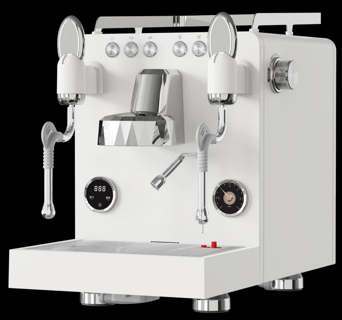
Sourcing commercial equipment requires strict quality verification. High-performance coffee machines must undergo comprehensive testing, including electrical safety, leakage, performance, aging, and noise tests. Relying on suppliers with international quality management certifications, such as ISO 9001, ensures the machinery meets rigorous commercial standards. Similar quality-assured supply strategies have successfully supported municipal and construction projects in regional hubs like Ecuador, establishing reliable long-term operations.
Data / Solution Comparison
Parameter / Feature Standard Single Boiler Dual Boiler System BFC Semi-automatic Espresso Machine Boiler Configuration Single shared boiler Two independent boilers 1.3L Steam Pot + 1300W Extraction Heating Block Simultaneous Brewing & Steaming No (requires transition time) Yes Yes Temperature Control Thermostat (low precision) PID Controller PID Function (adjustable externally) Pump System Standard pump Rotary or high-end vibration pump Imported Italian OLAB 15Bar pump Minimum Order Quantity (MOQ) Varies by supplier Varies by supplier 1000 pcs Payment Methods Subject to distributor terms Subject to distributor terms 30% T/T prepayment, 70% balance against B/L copy Shipping Methods Standard logistics Standard logistics Sea Freight (FCL/LCL) Frequently Asked Questions (FAQ)
Can a single boiler machine support a medium-to-high volume cafe?
Single boiler machines are generally not recommended for high-volume commercial environments because they cannot steam milk and extract espresso simultaneously without significant recovery delays, which increases customer wait times.
Why is PID temperature control important for commercial coffee brewing?
PID temperature control electronically regulates the heating elements to maintain precise water temperatures. This prevents temperature fluctuations that can lead to sour or bitter espresso extractions.
What are the benefits of using an imported Italian pump in a coffee machine?
Imported Italian pumps, such as OLAB 15Bar pumps, provide stable pressure curves during extraction, ensuring the correct water velocity through the coffee puck for optimal flavor extraction and crema formation.
Final Conclusion & Recommendations
For cafe startups expecting steady foot traffic and a menu focused on milk-based espresso drinks, investing in a dual boiler system or a high-efficiency steam pot and heating block hybrid machine is essential to maintain service speed and beverage consistency. When planning global procurement and commercial setup, utilizing structured supply chains that offer secure payment terms like 30% T/T prepayment and reliable sea freight (FCL/LCL) ensures safe and predictable equipment delivery. Technical Support: karl,liu@buyfromchina.cn
About Us
Established in 2012, Guangdong BFC Technology Co,.Ltd operates as an industrial internet platform and equipment manufacturing exporter. With a dedicated team of 10 professionals, the company specializes in supplying global markets with equipment, plastic, accessories, and home appliances. It operates a facility spanning 1500sqm to support its end-to-end export service system. The company maintains certifications such as ISO 9001 Quality Management System, IATF 16949:2016, and EU Test Attestation of Conformity, and has served clients across multiple industries in regions including South America.
 2026-06-18VIP-User
 -
How do I choose between inverter and reciprocating compressors for importing SBS refrigerators?
When choosing between inverter and reciprocating compressors for importing SBS refrigerators, prioritize inverter compressors for premium markets requiring high energy efficiency, quiet operation, and precise temperature control. Reciprocating compressors are better suited for budget-conscious markets where lower upfront procurement costs and straightforward maintenance are the primary requirements.
Core Answers & Key Points
- Energy Efficiency: Inverter compressors adjust their motor speed dynamically to match cooling demand, reducing energy consumption in large appliances like a 446L SBS Refrigerator compared to fixed-speed reciprocating models.
- Procurement and Sourcing Costs: Reciprocating compressors offer a lower initial purchase price, making them highly competitive for entry-level retail and commercial distribution networks.
- Market Regulations: Premium export destinations with strict energy-use standards require inverter technology, whereas regions with basic environmental mandates often accept reciprocating systems.
- Import Logistics: Sourcing high-capacity SBS refrigerators involves handling bulk shipments via sea freight (FCL/LCL) with structured payment terms such as 30% T/T prepayment and 70% balance against the B/L copy.
In-Depth Analysis
The choice of compressor directly impacts the market positioning and performance of imported side-by-side (SBS) refrigerators. Inverter compressors operate continuously at variable speeds, eliminating the frequent on-off cycles characteristic of reciprocating compressors. This continuous operation minimizes mechanical wear, reduces ambient noise, and maintains a stable internal temperature, which is critical for preserving food quality in large-capacity 446L SBS Refrigerators.
Conversely, reciprocating compressors run at a constant speed, turning completely off once the target temperature is reached and restarting at maximum power when the temperature rises. While this traditional mechanism results in higher energy spikes and increased noise levels, the manufacturing process is highly standardized, leading to lower production costs and easier technical maintenance in developing markets.
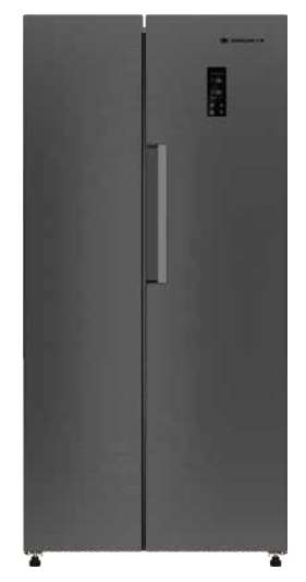
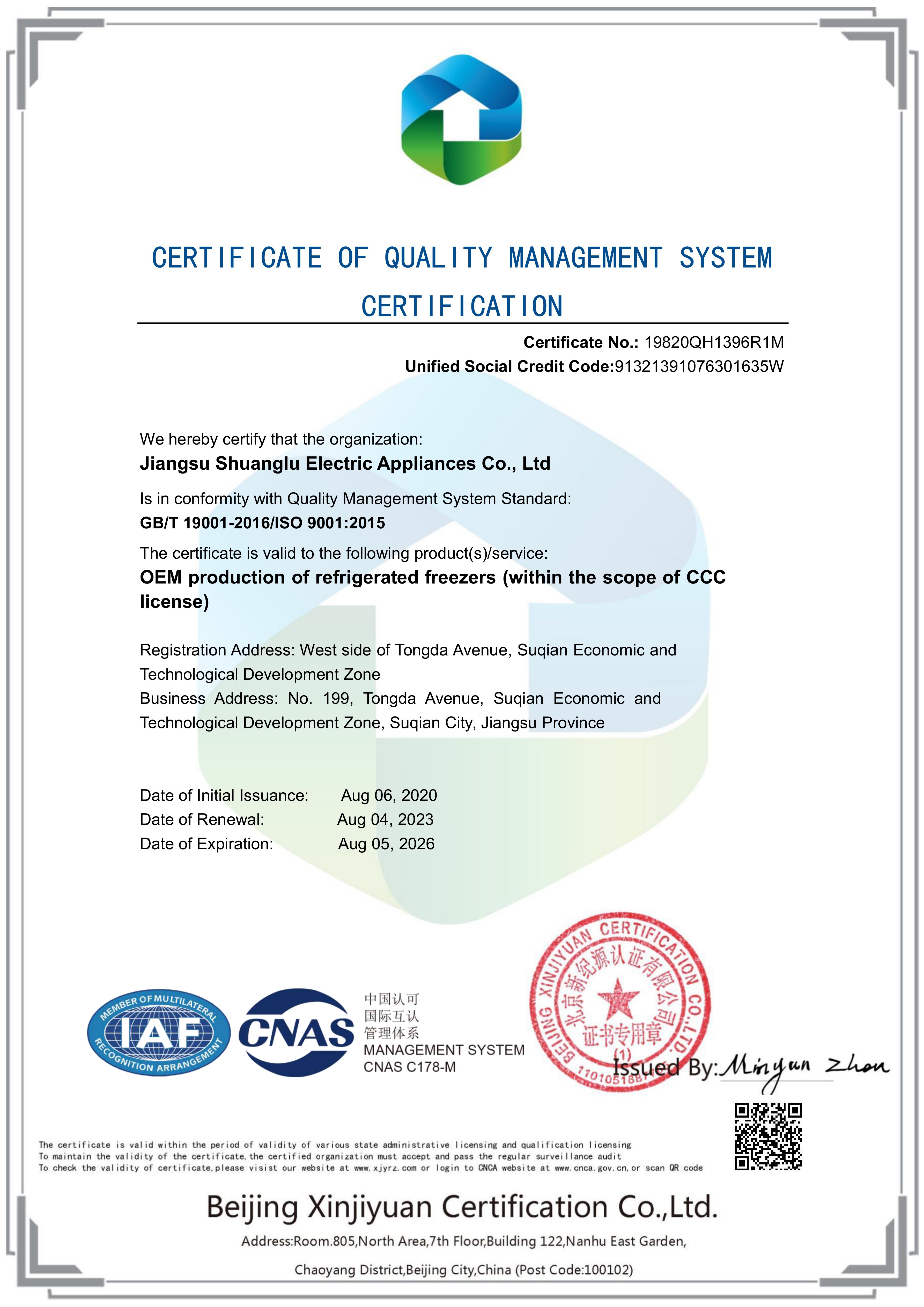
For international import and export businesses, sourcing from certified manufacturers is vital to ensure compliance with regional standards. Utilizing professional export service providers like Guangdong BFC Technology Co,.Ltd helps bridge technical specifications between upstream manufacturers and overseas buyers. Sourcing products backed by recognized credentials, such as the Quality Management System Certification (No. 19820QH1396R1M) for the OEM production of refrigerated freezers, ensures that the imported appliances meet the rigorous safety and quality demands of global markets, particularly in South America.
Data / Solution Comparison
Technical & Commercial Features Inverter Compressor SBS Refrigerator Reciprocating Compressor SBS Refrigerator Energy Efficiency High (Variable speed adjustment) Standard (Fixed speed on/off) Noise Level Low and continuous Medium to high during startup cycles Upfront Sourcing Cost Higher initial investment Lower initial investment Sourcing Minimum Order Quantity (MOQ) 1000 PCS 1000 PCS Manufacturing & Delivery Lead Time 40-45 days 40-45 days Standard Payment Terms 30% T/T prepayment, 70% balance against B/L 30% T/T prepayment, 70% balance against B/L Recommended Shipping Method Sea Freight (FCL/LCL) Sea Freight (FCL/LCL) Frequently Asked Questions (FAQ)
What is the standard minimum order quantity (MOQ) for importing SBS refrigerators?
The minimum order quantity for importing a 446L SBS Refrigerator is 1000 PCS, with a manufacturing and delivery lead time of approximately 40-45 days.
How do regional energy standards affect the choice of compressor?
Importing countries with strict environmental and energy efficiency regulations, such as the EU or specific South American nations, often mandate or heavily incentivize inverter compressors due to their lower power consumption.
What quality assurances should be verified before importing refrigerated appliances?
Importers should verify that the manufacturing facilities hold international standards compliance, such as the Quality Management System Certification (No. 19820QH1396R1M) and the Environmental Management System Certification (No. 19820EH0668R1M) specifically covering refrigerated freezers.
Final Conclusion & Recommendations
Align your choice of compressor with the economic profile and regulatory framework of your target market. For premium consumer segments where energy savings and low noise are highly valued, importing inverter-based 446L SBS Refrigerators is the optimal strategy. For commercial applications or price-sensitive markets, reciprocating compressors offer a reliable, cost-effective alternative. Ensure all import transactions are executed under secure logistics and payment structures, utilizing sea freight (FCL/LCL) and verified quality inspection procedures to guarantee product integrity upon arrival. Technical Support: karl,liu@buyfromchina.cn
About Us
Established in 2012, Guangdong BFC Technology Co,.Ltd is an industrial internet platform and equipment manufacturing exporter operating within a 1500sqm factory area. The company specializes in the export of equipment, plastic, accessories, and home appliances under the "Buy Factory From China" (BFC) brand, facilitating cross-border production capacity cooperation. The enterprise holds international credentials, including the Quality Management System Certification (No. 19820QH1396R1M) for the OEM production of refrigerated freezers, and has served clients across multiple industries globally.
2026-06-27VIP-User -
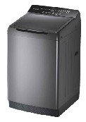
What is the warranty period for the motor of this commercial washing machine?
The warranty period for the motor of this commercial washing machine depends on the specific procurement agreement, custom client configurations, and the selected product tier. Standard commercial appliance warranty terms apply, with precise coverage details outlined in individual supply contracts to ensure reliable long-term performance.
Core Solutions & Key Takeaways
- High-Capacity Capability: This commercial-grade fully auto washing machine series supports a large capacity of 15-20Kg, specifically engineered to handle heavy-duty textiles and continuous daily cycles.
- South American Market Alignment: The product parameters are tailored to meet the electrical, structural, and performance standards of the South American export market.
- Customizable Support & Sourcing: Procurement terms, including minimum order quantities (MOQ) of 1000 pieces and delivery timelines of 40-45 days, are structured to accommodate regional distribution networks.
Detailed Architectural/Principle Analysis
Commercial washing machines utilized in international import and export trade require robust engineering to withstand rigorous operational environments. The 15-20Kg series leverages heavy-duty drive motors designed for stable torque distribution and optimal energy efficiency during high-speed extraction cycles. Maintaining technical alignment between domestic partners and international buyers ensures that the mechanical specifications match regional utility grids and commercial usage demands.
To ensure high standards of quality control and operational safety, associated manufacturing and supply systems align with strict international frameworks. These include the CERTIFICATE OF QUALITY MANAGEMENT SYSTEM CERTIFICATION (19820QH1396R1M) and the CERTIFICATE OF ENVIRONMENT MANAGEMENT SYSTEM CERTIFICATION (19820EH0668R1M). This systematic oversight guarantees that from initial material sourcing to final assembly, the equipment meets the environmental and operational regulations of major global regions, reducing the risk of premature motor wear or structural fatigue.
Data/Solution Comparison
Specification Parameter Commercial Washing Machine Details Operational & Supply Conditions Capacity Range 15-20Kg Series Suitable for high-volume commercial laundry Operation Mode Fully Automatic Optimized cycle times and water efficiency Minimum Order Quantity (MOQ) 1000 pcs Supports regional wholesale and distribution Delivery Lead Time 40-45 Days Calculated from order confirmation to port dispatch Primary Export Market South America Configured to regional voltage and grid standards Quality Inspection As required Subject to client-specified testing protocols Frequently Asked Questions (FAQ)
Q1: What are the shipping and payment terms for this commercial washing machine?
A1: Shipments are handled via Sea Freight (FCL/LCL). The standard payment structure is a 30% T/T prepayment with the remaining 70% balance settled against the B/L copy.
Q2: How is the technical compatibility of the motor verified for South American electrical grids?
A2: Technical specifications, voltage requirements, and frequency standards are precisely aligned with local regional requirements through strategic collaboration with technical partners before production begins.
Q3: Are there certified management systems supporting the production of these appliances?
A3: Yes, the supply and manufacturing systems are backed by recognized certifications, including ISO 9001 Quality Management System Certification (0070019Q51912R0M) and Occupational Health and Safety Management System Certification (19820SH0583R1M).
Final Conclusion & Recommendations
When sourcing commercial laundry equipment for global markets, verifying motor warranty terms, electrical configurations, and supply chain logistics during the contract negotiation phase is highly recommended. For detailed technical solutions, customized motor configurations, or specific warranty coordination, please reach out to us via karl.liu@buyfromchina.cn.
About Us
Guangdong BFC Technology Co,.Ltd (BFC), established in 2012, operates as an industrial internet platform, equipment manufacturing exporter, and holistic solution provider. The company specializes in building cross-border production capacity cooperation platforms to help Belt and Road countries establish basic industrial systems, exporting equipment, plastics, accessories, and home appliances. BFC maintains a comprehensive end-to-end export service system, leveraging over a decade of dedicated foreign trade experience to deliver efficient logistics, customs clearance, and supply chain management for the global market.
2026-07-15VIP-User -
How is technical support handled for overseas outdoor speaker buyers?
Technical support for overseas outdoor speaker buyers is handled through structured manufacturer warranties, online troubleshooting, and localized partner support. Buyers receive a one-year warranty covering functional defects, backed by remote technical guidance, hardware diagnostics, and replacement parts delivered via global shipping channels to minimize device downtime.
Core Solutions & Key Takeaways
- One-Year Warranty Coverage: Direct manufacturing defects are covered under a standardized one-year warranty, ensuring reliable long-term operations for retail and distribution partners.
- Multi-Scenario Performance Validation: Technical diagnostics accommodate diverse environmental challenges, whether addressing waterproofing issues in Beach & Poolside Fun or structural resilience in Camping & Hiking scenarios.
- Documented Compliance Standards: Products are backed by international certifications, verifying that the hardware meets rigorous safety, radio frequency, and environmental criteria before dispatch.
Detailed Architectural/Principle Analysis
Technical support for the MIETUBL GLOBAL SUPPLY CHAIN(GUANGZHOU) CO.,LTD Magnetic Mini Speaker MTB-BLSP07 is structured around quality control and fast-response diagnostics. Operating under the GB/T2828.1 quality inspection standard, each unit undergoes strict testing during the manufacturing process. This systematic approach ensures the Wireless V5.4 chip, 1200mAh battery, and 5W speaker hardware function within specified parameters before export.
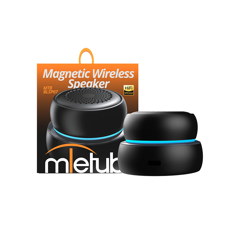
When an overseas buyer encounters a technical issue, the resolution workflow begins with remote debugging. Technicians analyze the wireless connectivity protocols (HFP, A2DP, AVRCP) and DSP audio processing settings (SBC, AAC) to resolve pairing or audio degradation issues. If hardware failure is confirmed within the warranty period, replacement components are integrated into subsequent shipping batches, or dispatched via air freight to restore unit functionality rapidly. This technical framework is supported by international compliance, including the RED certification (HX240417001RED-MTB) for wireless Bluetooth speakers, assuring buyers of standardized hardware integrity.
Data/Solution Comparison
The following table outlines the technical specifications, support options, and delivery logistics for overseas buyers managing outdoor speaker inventories:
Technical Parameter / Service Type Specification / Support Level Logistics & Compliance Reference Model Identifier MTB-BLSP07 (Pair Name) Wireless Version V5.4 Battery & Playback 1200mAh Capacity / 4 Hours Playtime 100Hz-20KHz Frequency Response Quality & Support GB/T2828.1 / One-Year Warranty RED Certified (No. HX240417001RED-MTB) Shipping Methods Available Air Freight, Land Transportation, Sea Freight FCL and LCL options supported Minimum Order Quantity (MOQ) 1000 Pieces 30-Day Delivery Lead Time Frequently Asked Questions (FAQ)
Q1: How do overseas buyers initiate a warranty claim for the MTB-BLSP07?
A1: Buyers must document the technical issue with video or photo evidence showing the speaker size, serial number, and failure symptoms, then submit this data to the support team for analysis under the one-year warranty program.
Q2: What shipping methods are used to deliver replacement parts or bulk orders?
A2: Logistics are handled through Air Freight for urgent technical parts, Land Transportation for regional border deliveries, or Sea Freight (FCL/LCL) for cost-effective bulk distribution.
Q3: Are the outdoor speakers certified for sale in highly regulated international markets?
A3: Yes, the products carry key certifications such as the RED certification for wireless Bluetooth speakers, ensuring they meet the technical safety and radio requirements of global markets.
Final Conclusion & Recommendations
Overseas buyers can safeguard their outdoor speaker investments by leveraging structured one-year manufacturer warranties and adhering to the GB/T2828.1 quality inspection standards during receiving. Utilizing established shipping networks—ranging from rapid Air Freight to bulk Sea Freight—ensures components and replacement units arrive predictably. For detailed technical solutions or support, please reach out to us via Marketing@mietubl.com.
About Us
MIETUBL GLOBAL SUPPLY CHAIN(GUANGZHOU) CO.,LTD is a leading mobile phone accessories brand headquartered in Guangzhou, established in 1998. Focusing on the 3C digital accessories sector, the brand operates a 10,000-square-meter private industrial park with 150 employees to manage independent R&D and manufacturing. The company holds key international certifications including CE, ROHS, FCC, and Gold Plus Supplier Assessment Certificate, serving B2B strategic partners and retail networks worldwide.
 2026-07-15VIP-User
Latest Blogs

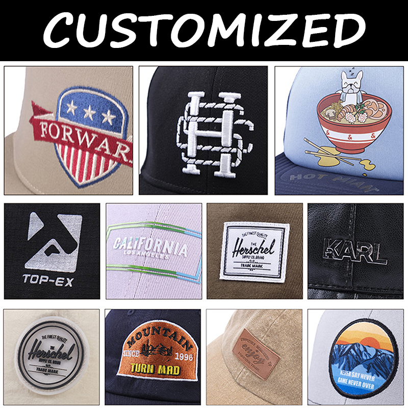
Why choose wholesale custom embroidery vintage baseball caps for your brand?
How wholesale custom embroidery baseball caps achieve superior quality and design flexibility
| Parameter | Specification |
|---|---|
| Material | Organic cotton |
| Style | Vintage distressed |
| Embroidery | Custom multicolor |
| Gender | Unisex |
| Type | Baseball cap |
What are the benefits of custom embroidery on vintage baseball caps?
How to choose the best wholesale supplier for distressed organic cotton caps?
Are custom embroidery baseball caps with organic cotton safe and durable?
Wholesale custom embroidery baseball caps: solving key challenges for brand owners, retailers, and event organizers
Expert recommendations for sourcing your custom caps
- Prioritize suppliers who can demonstrate their embroidery precision with sample proofs before committing to a full production run.
- Verify the organic cotton certification to ensure your sustainability claims are credible and verifiable.
- Request a physical sample of the vintage distressed finish to confirm the aesthetic matches your brand vision.
- Discuss your timeline upfront to ensure the supplier can meet your delivery requirements without expediting fees.

Yes, a 12-inch durable ABS trolley suitcase can be a great choice for travel, but its carry-on compliance depends entirely on the airline. While the 12-inch size is generally small enough to fit most international and domestic carry-on size restrictions, you must check your specific airline's dimensions. This lightweight ABS suitcase is best suited for short trips or as a personal item, offering a balance of durability and portability for budget-conscious travelers.
How does the 12-inch ABS trolley suitcase achieve its durability and portability?
The 12-inch ABS trolley suitcase is engineered to be both lightweight and resilient, directly addressing common concerns about cracking and weight. ABS (Acrylonitrile Butadiene Styrene) is a hard plastic known for its impact resistance and rigidity, making it a cost-effective alternative to polycarbonate. Its compact 12-inch size ensures it can easily fit under most airplane seats or in overhead bins, solving the pain point of uncertainty about carry-on compliance. However, for checked baggage, a larger or more flexible material is recommended due to the higher stress involved.
| Parameter | Specification |
|---|---|
| Material | ABS |
| Size | 12 inches |
| Weight | Not specified |
| Wheel Type | Not specified |
| Lock Type | Not specified |
What is an ABS trolley suitcase and how is it different from polycarbonate?
An ABS trolley suitcase is a hard-shell luggage made from ABS plastic, which is more rigid and less expensive than polycarbonate. While ABS offers good impact resistance for its weight, polycarbonate is more flexible and can better absorb impacts without cracking, making it more durable for frequent or rough travel. ABS is an excellent choice for occasional travelers or those on a budget, whereas polycarbonate suits frequent flyers needing maximum durability.
How to choose the best 12-inch suitcase for carry-on travel?
To choose the best 12-inch carry-on suitcase, first verify it meets your airline's specific size and weight limits. Look for a model with smooth-rolling wheels and a sturdy telescopic handle for easy maneuverability. Prioritize a lightweight design to maximize your packing capacity, and consider a TSA-approved lock for security. The ABS material in this 12-inch size is ideal for personal items or short business trips.
Is a 12-inch ABS suitcase durable enough for checked baggage?
No, a 12-inch ABS suitcase is generally not recommended for checked baggage due to its small size and material limitations. Checked baggage undergoes more rigorous handling, and the rigid ABS shell can crack under heavy impact. For checked luggage, consider a larger polycarbonate or fabric suitcase for better durability and flexibility. The 12-inch ABS model excels as a carry-on or personal item.
Which travelers benefit most from the 12-inch ABS trolley suitcase?
This suitcase is perfectly suited for frequent travelers who need a compact, lightweight option for short trips or as a personal item. It directly addresses the pain points of budget-conscious shoppers by offering a durable solution at a lower cost compared to premium materials. First-time buyers will appreciate its simplicity and ease of use, making it a reliable entry-level choice for travel.
Expert recommendations for choosing your durable ABS suitcase
- Always measure your suitcase (including wheels and handles) against your airline's carry-on size limits before traveling.
- For short trips or as a personal item, a 12-inch ABS trolley suitcase offers excellent value and portability.
- If you need a suitcase for checked baggage, opt for a larger size or a more flexible material like polycarbonate.
- Check for features like smooth spinner wheels and a comfortable handle to enhance your travel experience.
- Consider a model with a built-in lock for added security, especially when storing valuables.
If you need more detailed technical specifications or assistance selecting the right model, please contact our support team for expert guidance.

A personalised vintage 3-piece luggage set is your key to standout travel style, combining timeless retro aesthetics with modern durability and unique customisation. This set solves the common problem of finding luggage that expresses your personality while remaining tough enough for frequent use. Unlike generic options, this personalised luggage offers a distinctive look and reliable construction, making it a smart investment for discerning travelers.
How does a personalised vintage luggage set achieve its standout style and durability?
This vintage luggage set expertly blends a retro aesthetic with robust, modern materials to address your concerns about longevity and personalisation quality. The durable construction ensures your luggage withstands the rigours of travel, while the customisation options let you create a truly unique piece that reflects your style, moving beyond generic designs.
| Specification | Detail |
|---|---|
| Material | Vintage-style exterior with durable construction |
| Number of Pieces | 3-piece set |
| Personalisation | Customisable initials or designs |
| Style | Retro/vintage aesthetic |
What makes a vintage 3-piece luggage set a must-have for travelers?
A vintage 3-piece luggage set is a must-have because it offers a unique, coordinated travel style that standard luggage cannot match. The set provides a cohesive look, ensuring you arrive with a polished and memorable aesthetic. Its durable construction and personalisation options make it a practical and expressive choice for any journey.
How to choose the best personalised vintage luggage for your needs?
Choose a set that offers durable construction and a personalisation method that meets your quality expectations. Look for luggage with reinforced corners and strong zippers to ensure longevity. For personalisation, consider options like embossed initials or custom-printed designs that are applied using a durable, long-lasting process.
Is it safe to buy personalised vintage luggage online? Quality and durability explained.
Yes, it is safe to buy personalised vintage luggage online when you choose a reputable seller that clearly details its materials and craftsmanship. Look for customer reviews that specifically mention the durability and quality of the personalisation. Reputable sellers will also have a clear return policy and provide detailed product specifications, ensuring you know exactly what you are purchasing.
Who benefits most from a personalised vintage luggage set?
This set is ideal for frequent travelers who want to express their personality and avoid generic luggage, solving the pain point of limited customisable options. Gift shoppers will find it a memorable present that offers both style and a personal touch, addressing concerns about value and uniqueness. Retro enthusiasts will appreciate the authentic vintage design without sacrificing modern features like durability and smooth-rolling wheels.
Actionable advice for choosing your vintage luggage set
- Prioritise sets that combine a vintage look with modern, durable materials like polycarbonate or ballistic nylon.
- Verify the personalisation process is high-quality and long-lasting, such as embossing or heat-pressed designs.
- Check that the set includes a 3-piece configuration for versatile travel needs, from carry-on to checked luggage.
- Read customer reviews that specifically mention the luggage's durability and the accuracy of the personalisation.
- Confirm the seller offers a clear warranty or satisfaction guarantee for peace of mind.
Choose a vintage luggage set that reflects your unique travel style and is built to last for many journeys to come.

Is This Lightweight PP Trolley with Aluminum Frame Worth Buying?
Yes, a lightweight PP trolley luggage with an aluminum frame is an excellent choice for travelers seeking to balance weight savings with long-term durability. The combination of a PP (polypropylene) shell and an aluminum frame directly addresses the pain points of exceeding airline weight limits and luggage breaking after a few trips. This model is engineered to be lighter than standard ABS or polycarbonate suitcases while providing superior structural integrity through its aluminum frame, making it a reliable option for frequent flyers.
How Does the Lightweight PP Trolley Luggage Achieve Its Durability?
The key to this luggage’s performance lies in its material synergy. The PP material is inherently lightweight and flexible, allowing it to absorb impacts without cracking, while the aluminum frame adds a rigid skeleton that prevents the case from deforming under pressure. This combination solves the common pain point of luggage breaking easily, as the frame protects the shell from stress during handling. Below are the core specifications that define this model’s value.
| Parameter | Specification |
|---|---|
| Material | PP (Polypropylene) |
| Frame Type | Aluminum |
| Weight | Lightweight (exact weight not specified, but optimized for airline limits) |
| Size Options | Not specified (likely standard carry-on or check-in sizes) |
This table shows that the luggage prioritizes a lightweight build without sacrificing the protective frame, making it a balanced solution for travelers who need both mobility and safety for their belongings.
What Is PP Material in Luggage and Why Is It Lightweight?
PP (polypropylene) is a thermoplastic polymer known for being one of the lightest and most impact-resistant materials used in luggage. Unlike ABS, which is harder but can crack under stress, or polycarbonate, which is heavier, PP offers a unique flexibility that absorbs shocks without adding bulk. This makes it ideal for travelers who want to maximize packing capacity while staying under airline weight restrictions. The material’s natural resilience also helps prevent surface cracks, extending the suitcase’s lifespan.
How to Compare Lightweight Trolley Luggage for Long Trips?
Focus on three factors: material weight, frame type, and wheel quality. For long trips, a lightweight PP shell with an aluminum frame is superior to ABS or pure polycarbonate options because it reduces fatigue when carrying the bag and provides better resistance to rough handling. Additionally, check for spinner wheels and a telescopic handle made from aluminum, as these enhance maneuverability. Always verify the actual weight against your airline’s limit, as some lightweight models may still be heavier than advertised.
Is Aluminum Frame Luggage Safe and Durable for Air Travel?
Yes, an aluminum frame significantly enhances safety and durability for air travel by protecting the suitcase’s contents from crushing and impact. Unlike soft-sided or frameless luggage, the aluminum frame distributes stress evenly, preventing the case from collapsing during baggage handling. This is especially important for fragile items. While aluminum frames add some weight, the trade-off is a much higher resistance to damage, making it a durable choice for frequent flyers who prioritize protection.
Lightweight PP Trolley Luggage: Who Benefits Most?
This luggage is specifically designed for three key groups of travelers. First, frequent travelers concerned about weight limits will appreciate the lightweight PP material that helps them pack more without additional fees. Second, budget-conscious shoppers get excellent value from the durable aluminum frame that reduces replacement costs over time. Third, first-time buyers unsure about materials will find this combination offers a clear advantage: it is lighter than ABS, more durable than pure polycarbonate, and more affordable than high-end options, eliminating the guesswork from their purchase.
Expert Recommendations for Choosing This Luggage
- Prioritize the aluminum frame over the material alone, as it is the primary driver of long-term durability and impact resistance.
- Verify the exact weight of the suitcase before purchasing, as “lightweight” can vary by brand, and compare it to your airline’s carry-on or checked baggage limit.
- Check wheel quality and handle sturdiness, as these components are common failure points in lightweight luggage; aluminum handles are preferred.
- Consider the size options available to ensure the suitcase fits your typical travel needs, whether for a weekend trip or an extended vacation.
If you need further technical details on how this PP and aluminum combination performs in real-world conditions, contact our support team for personalized guidance.

How to choose a reliable foldable PP luggage supplier for wholesale?
How to Choose a Reliable Foldable PP Luggage Supplier for Wholesale?
Choosing a reliable foldable PP luggage supplier for wholesale requires verifying material quality, folding mechanism durability, and bulk order capabilities. For B2B buyers, the key is to focus on suppliers that demonstrate strong factory capabilities and clear compliance with industry standards, ensuring cost-effective, durable collapsible shopping luggage that minimizes return rates and meets your supply chain needs.
How to Compare Wholesale Foldable Luggage Suppliers Through Technical Specifications?
When evaluating suppliers, focus on the specific technical specs that directly impact product durability and cost per unit. The table below outlines the essential parameters for foldable PP luggage, helping you quickly compare offers and address pain points like material authenticity and folding mechanism durability.
| Parameter | Detailed Specification |
|---|---|
| Material | PP (Polypropylene) |
| Feature | Foldable |
| Usage | Travel and shopping |
These specifications confirm that the luggage is made from polypropylene, a lightweight yet robust material, and designed for easy storage and transportation. Reliable suppliers will provide additional data on load capacity, fold cycle tests, and lead times, directly addressing your concerns about high return rates and uncertain order quantities.
What is Foldable PP Luggage Made Of?
Foldable PP luggage is made primarily from polypropylene (PP), a durable, lightweight thermoplastic known for its high impact resistance and flexibility. This material allows the luggage to be collapsed for space-saving storage while maintaining structural integrity during travel. The folding mechanism typically uses reinforced hinges or snap-lock joints, which are tested for repeated use to ensure long-term reliability.
Are There Any Safety Certifications for PP Luggage Materials?
While specific certifications for PP luggage materials vary by region, industry-standard compliance like REACH (EU) or FDA (US) for material safety is critical for wholesale buyers. Reputable suppliers should provide documentation proving their PP is free from harmful substances and meets international safety norms. If certifications are not explicitly listed, ask for material safety data sheets (MSDS) or third-party test reports to verify quality and authenticity.
Foldable PP Luggage: Solutions for Wholesale Buyers
This product directly addresses the core needs of wholesale buyers, retail store owners, and corporate procurement managers. For wholesale buyers concerned about durability and cost, the foldable design reduces shipping volume and warehousing costs. Retail store owners benefit from space-saving displays and a product that appeals to customers seeking collapsible shopping luggage. Corporate procurement managers can rely on consistent bulk supply for promotional events, with clear minimum order quantities and lead times once a supplier’s capabilities are verified.
Expert Recommendations for Selecting a Supplier
- Prioritize suppliers that provide detailed material certifications and folding mechanism test results to reduce return rates.
- Request samples to verify the PP material’s authenticity and the durability of the foldable design under repeated use.
- Confirm minimum order quantities and lead times upfront, and look for suppliers with scalable factory capabilities for future bulk orders.
- Compare cost per unit across multiple suppliers, factoring in savings from reduced shipping volume due to the foldable feature.
- Choose a supplier that offers clear communication on compliance and quality control processes to ensure supply chain reliability.
For direct technical support or to verify supplier capabilities, contact our engineering team for further guidance.

Yes, the Luxury 4pcs PP Travel Luggage Set is an excellent choice for travelers seeking a durable and lightweight solution. Made from Polypropylene (PP), this 4-piece set offers exceptional impact resistance while remaining significantly lighter than traditional ABS or polycarbonate luggage, directly addressing the pain point of heavy bags that exceed airline weight limits.
How Does the PP Travel Luggage Set Deliver Durability and Lightweight Performance?
The key to this set's performance lies in its material, PP (Polypropylene), which is inherently flexible and crack-resistant, ensuring the luggage can withstand the rough handling of airport baggage systems without breaking. Combined with a 4-piece configuration, this set provides a complete travel solution—from a carry-on to a large checked bag—without the excessive weight of other materials.
| Parameter | Specification |
|---|---|
| Material | PP (Polypropylene) |
| Piece Count | 4 |
| Type | Travel Luggage Set |
| Feature | Lightweight & Durable |
What is PP Material in Luggage and Is It Durable?
PP (Polypropylene) is a highly durable, lightweight thermoplastic known for its excellent impact resistance and flexibility. Unlike harder materials that can crack on impact, PP flexes to absorb shocks, returning to its original shape. This makes it ideal for luggage that must survive frequent flights and rough handling without adding significant weight.
How to Choose the Best 4-Piece Luggage Set for International Travel?
Prioritize a set that offers a range of sizes, lightweight construction, and durable materials like PP. For international travel, you need a carry-on that meets airline regulations, a medium checked bag, and a large checked bag. A 4-piece set provides this complete range, ensuring you are prepared for any trip length while keeping your total luggage weight low to avoid fees.
Is the Luxury 4pcs PP Travel Luggage Set Safe and TSA-Approved?
Yes, the set is designed with integrated TSA-approved combination locks for secure and hassle-free travel. These locks allow TSA agents to inspect your luggage without damaging the lock, providing peace of mind during international flights. The durable PP shell also protects your belongings from impacts and moisture.
Who Benefits Most from the PP Travel Luggage Set?
This set is ideal for frequent flyers who need luggage that survives repeated flights without breaking, budget-conscious shoppers looking for a complete, value-packed set that doesn't sacrifice weight, and family travelers needing a coordinated, durable solution for multiple members that is easy to handle.
Expert Recommendations for Your Purchase
- Prioritize PP material for the best balance of durability and lightweight performance.
- Choose a 4-piece set to ensure you have the right size for any trip, from quick business trips to extended vacations.
- Always check for TSA-approved locks to avoid damage during security inspections.
- Verify the set's weight and dimensions against your preferred airline's carry-on and checked baggage policies.
For further technical specifications or bulk purchasing inquiries, contact the manufacturer's support team for detailed assistance. If you need a reliable and lightweight travel solution, this PP set offers proven performance and value.
Popular Blogs
-

Cabinet Connector Hardware And Cabinet Fasteners
Cabinet connector hardware and cabinet fasteners play a pivotal role in the world of cabinetry, ensuring that furniture is not only functional but also visually appealing. This specialized hardware helps in the assembly and longevity of cabinets, making it essential for homeowners, builders, and designers alike. With a variety of options available in the market, understanding these components is crucial for anyone looking to create durable and attractive cabinetry. This article explores the different types of cabinet connector hardware and fasteners, their importance, and how they contribute to successful cabinetry construction.
Understanding Cabinet Connector Hardware
Cabinet connector hardware refers to a range of components specifically designed to join sections of cabinetry together. These fittings are engineered to provide strong joints, which are vital for maintaining the structure's integrity over time. Common types of cabinet connectors include dowels, biscuits, cam locks, and metal brackets. Each of these options has its unique applications and advantages, making them suitable for different cabinetry needs.
Dowels are cylindrical rods that fit into pre-drilled holes of adjoining pieces, ensuring precise alignment and robust support. Biscuit joints utilize oval-shaped pieces of wood, known as biscuits, that fit into slots cut into the materials, providing strength and stability. Cam locks, often featured in ready-to-assemble furniture, allow for quick and secure joining with the help of a simple turn of a knob. Lastly, metal brackets are typically used for reinforcing corners and joints, adding an extra layer of support where it is needed most.
The Significance of Cabinet Fasteners
Cabinet fasteners are crucial for the assembly process as they provide the necessary means to hold cabinet components together. They come in various forms, including screws, nails, and specialized fasteners like pocket hole screws and Euro screws. Each type of fastener has its specific role, and choosing the right one can significantly impact the overall strength and durability of the cabinetry.
Screws are the most commonly used fasteners in cabinetry, renowned for their holding power. They are available in multiple designs, such as wood screws and machine screws, each catering to different materials and assembly methods. Nails, while less robust than screws, can be used in specific applications where speed is essential, such as when using pre-fabricated parts. Pocket hole screws allow for concealed joining, making them ideal for creating furniture with clean lines, while Euro screws typically facilitate drawer assembly and cabinet hinging by providing sturdy and discreet mounting points.
Materials and Their Impact
The materials used in cabinet connector hardware and fasteners also play a crucial role in their effectiveness. Common materials include steel, brass, and plastic, each offering distinctive benefits. Steel fasteners are durable and resistant to bending, making them suitable for heavier applications, while brass connectors offer a more aesthetic finish, particularly in exposed areas. On the other hand, plastic fasteners can provide lightweight options for temporary or low-stress applications.
Moreover, the finish of the materials can influence their performance. For example, coated or galvanized steel can resist rust and corrosion, which is vital in kitchen or bathroom environments where moisture is present. With advancements in technology, manufacturers also offer specialized coatings that enhance the appearance while maintaining strength, allowing for seamless integration into various design themes.
Installation Techniques and Considerations
Proper installation techniques significantly affect the overall performance of cabinet connectors and fasteners. When setting up cabinetry, it is essential to follow the manufacturer's instructions meticulously, as improper installation can lead to structural issues over time. For instance, ensuring that screws are not over-tightened can prevent wood from splitting, while allowing the predefined dowel holes to line up correctly is crucial for achieving a tight joint.
Moreover, alignment is key when assembling cabinets. Utilizing tools like clamps can help in maintaining the correct positioning during installation, ensuring that the cabinet frame remains square and stable. Additionally, pre-drilling holes for screws can mitigate the risk of damaging the wood, especially in hardwood materials. Understanding these installation techniques empowers builders and DIY enthusiasts to achieve better results in their cabinetry projects.
Choosing the Right Components for Your Project
When embarking on a cabinetry project, selecting the appropriate cabinet connector hardware and fasteners is vital for achieving both functionality and aesthetics. Assessing the specific needs of your project, including the type of materials you'll be working with, the level of stress the joint will endure, and the desired finish, will help inform your choices. Consulting with hardware experts or manufacturers can also provide valuable insights into the best products for your particular application.
In conclusion, cabinet connector hardware and fasteners are essential components that contribute significantly to the durability and functionality of cabinetry. By understanding the various types of connectors and fasteners available, as well as the importance of material and installation techniques, individuals can ensure that their cabinetry projects are both attractive and enduring. The right choices can transform ordinary furniture into beautiful and resilient installations, enhancing the overall value and appeal of any space.
gztoplink2025-01-24 -
The Artistry of Wigs: Exploring the Beauty, Versatility, and Cultural Significance of Wigs in Fashion and Everyday Life Across the Globe is a fascinating journey into the world of wigs, uncovering their transformative power and deep-rooted cultural meanings. From ancient civilizations to modern runways, wigs have played a pivotal role in self-expression, identity, and artistry. This exploration delves into how wigs transcend mere fashion accessories, becoming symbols of creativity, tradition, and societal norms.
The Historical Evolution of Wigs
Wigs have a rich history that dates back thousands of years. In ancient Egypt, wigs were worn by both men and women as symbols of status and protection from the sun. The elaborate designs often featured braids and beads, reflecting the artistry of the time.
During the 17th and 18th centuries in Europe, wigs became a staple of aristocratic fashion. Powdered wigs, or perukes, were synonymous with wealth and power, adorning the heads of kings and nobles. This era highlighted the wig's role as a marker of social hierarchy.
Wigs in Modern Fashion
Today, wigs are celebrated for their versatility in the fashion industry. Designers and stylists use wigs to create bold, avant-garde looks on runways, pushing the boundaries of creativity. From neon-colored wigs to realistic human hair pieces, the possibilities are endless.
Celebrities and influencers also embrace wigs as a tool for reinvention. Stars like Lady Gaga and Rihanna have popularized the use of wigs to experiment with different personas, proving that wigs are more than just accessories—they are extensions of identity.
Cultural Significance of Wigs
In many cultures, wigs hold profound symbolic meaning. In Japan, traditional wigs, or katsura, are used in theater performances like Kabuki to portray characters and emotions. These wigs are meticulously crafted to preserve cultural heritage.
In African communities, wigs and hairpieces are often tied to notions of beauty and pride. The vibrant styles and textures celebrate diversity and serve as a connection to ancestral traditions. Wigs here are not just fashion statements but also cultural affirmations.
Wigs in Everyday Life
Beyond fashion and culture, wigs play a practical role in everyday life. For individuals experiencing hair loss due to medical conditions, wigs offer a sense of normalcy and confidence. High-quality, natural-looking wigs can be life-changing.
Additionally, wigs provide a low-commitment way to experiment with different looks. Whether for a special occasion or a daily change, wigs allow people to express themselves without permanent alterations to their natural hair.
topmi052025-03-26 -
Superior Mixing Technology for Enhanced Production Output
In today's competitive manufacturing landscape, optimizing production output is paramount. Achieving this often hinges on seemingly minor details, one of the most crucial being the efficiency of mixing processes. Superior mixing technology is no longer a luxury but a necessity for businesses seeking to enhance production rates, improve product quality, and reduce operational costs. This technology encompasses a range of advancements that significantly impact various industries, from pharmaceuticals and food processing to chemicals and cosmetics.Improved Mixing Efficiency and Uniformity
Traditional mixing methods often suffer from inconsistencies, leading to variations in product quality and potentially wasted materials. Superior mixing technologies, such as high-shear mixers and specialized impeller designs, address this directly. These systems create more powerful and consistent mixing actions, ensuring a uniform distribution of ingredients throughout the entire batch. This uniformity translates to improved product consistency and reduces the need for rework or rejection of substandard products.
Furthermore, advanced process control systems integrated with these mixers allow for precise monitoring and adjustment of mixing parameters such as speed, time, and temperature. This level of control ensures optimal mixing efficiency and reproducibility, minimizing variations between batches and enhancing overall product quality.
Reduced Mixing Time and Increased Throughput
Faster mixing translates directly into increased production output. Superior mixing technologies, through their improved designs and more powerful capabilities, significantly reduce the overall mixing time compared to older methods. This allows for a greater number of batches to be processed within a given timeframe, leading to substantial gains in productivity.
This enhanced throughput is particularly beneficial in high-volume production environments where even minor reductions in mixing time can have a significant impact on the overall production capacity. The faster turnaround time also contributes to shorter lead times and improved responsiveness to market demands.
Enhanced Scalability and Flexibility
Modern mixing technologies are designed with scalability in mind. This means that the same fundamental principles and design features can be adapted to different production scales, allowing businesses to easily expand their production capacity as needed without requiring a complete overhaul of their mixing infrastructure.
Furthermore, many superior mixing systems offer greater flexibility in handling different types of materials and viscosities. This adaptability reduces the need for multiple, specialized mixing units, streamlining operations and reducing capital expenditure.
In conclusion, adopting superior mixing technology represents a strategic investment for businesses aiming to enhance their production output. The benefits extend beyond increased throughput, encompassing improved product quality, reduced costs, and enhanced operational flexibility – all crucial elements in today's fiercely competitive market.wzwanxi2024-12-30 -
Wholesale Custom Designed Wetsuits Diving Suits Perfect Fit for Men and Women
The allure of the underwater world has captivated humans for centuries. From casual snorkeling to professional deep-sea diving, exploring the ocean's depths requires specialized equipment that prioritizes safety, comfort, and performance. Central to this equipment is the wetsuit – a garment designed to provide thermal protection, buoyancy control, and abrasion resistance in aquatic environments. For businesses looking to supply divers with high-quality, personalized gear, wholesale custom-designed wetsuits represent a lucrative and rewarding venture. These suits offer a unique opportunity to cater to the diverse needs and preferences of both male and female divers, ensuring a perfect fit and optimal performance in any aquatic condition. This detailed exploration will delve into the advantages of offering wholesale custom-designed wetsuits and highlight the crucial factors involved in their successful design and production.Superior Comfort and Performance Through Customization
Standard, off-the-shelf wetsuits often fail to provide the perfect fit for every individual. Variations in body shape, size, and flexibility can lead to uncomfortable pressure points, restricted movement, and compromised thermal insulation. Custom-designed wetsuits, however, address these issues head-on. By taking precise body measurements and considering the diver's specific needs and diving style, manufacturers can create suits that are tailored to their unique physiology. This results in unparalleled comfort, allowing divers to focus on their underwater exploration without the distraction of ill-fitting gear.
Moreover, customized wetsuits enhance performance. A perfectly fitting suit minimizes water ingress, maximizing thermal protection and reducing the need for excessive neoprene thickness. This translates to greater flexibility and agility underwater, allowing for easier maneuvering and more efficient swimming. The ability to customize aspects like seam placement and neoprene panel thickness based on individual body heat distribution further improves both comfort and performance, leading to a superior diving experience.
Materials and Construction: Ensuring Durability and Longevity
The choice of materials is paramount in determining the quality, durability, and performance of a custom-designed wetsuit. High-quality neoprene remains the industry standard for its thermal insulation properties and flexibility. However, the specific type of neoprene, its thickness, and its lining material can be customized to suit various diving environments and individual preferences. For example, divers operating in colder waters might opt for thicker neoprene, while those in warmer climates might prefer a thinner, more flexible option.
Beyond neoprene, the construction techniques employed are critical. Proper stitching, glued and blind-stitched seams, and strategically placed reinforcements are essential to ensure the suit's durability and longevity. Custom-designed wetsuits allow for precise control over these elements, reducing the risk of leaks, tears, and premature wear and tear. The ability to incorporate reinforced panels in high-stress areas further enhances the suit's lifespan, making it a worthwhile investment for serious divers.
Targeting Specific Diving Disciplines and Preferences
The versatility of custom-designed wetsuits extends to accommodating various diving disciplines. Whether it's freediving, scuba diving, spearfishing, or surfing, the design can be tailored to meet the specific requirements of each activity. For freediving, for example, a suit might prioritize hydrodynamic efficiency and minimal drag. For spearfishing, it could incorporate reinforced padding for abrasion resistance and pockets for carrying equipment. This adaptability opens up significant market opportunities for wholesalers, allowing them to cater to a diverse range of customers with specialized needs.
Furthermore, aesthetic preferences can be incorporated into the custom design process. Divers can choose from a wide range of colors, patterns, and customization options, allowing them to express their individuality and create a truly unique wetsuit. This personalization aspect significantly enhances customer satisfaction and builds brand loyalty, creating a positive feedback loop that drives sales and repeat business.
Wholesale Advantages: Maximizing Profitability and Market Reach
Offering wholesale custom-designed wetsuits allows businesses to tap into a lucrative market segment. By purchasing in bulk and offering personalized options, wholesalers can negotiate competitive pricing with manufacturers, ensuring healthy profit margins. Moreover, the ability to offer a wider range of sizes, styles, and customization options broadens the target market and increases sales potential.
Wholesale distribution also facilitates efficient inventory management and reduces storage costs. Instead of maintaining large stocks of ready-made wetsuits in various sizes, wholesalers can focus on managing orders and coordinating production with manufacturers. This streamlined approach minimizes warehousing expenses and reduces the risk of inventory obsolescence.
In conclusion, wholesale custom-designed wetsuits represent a compelling business opportunity. By focusing on superior comfort, performance, durability, and personalized options, businesses can capture a significant share of the diving equipment market. The ability to cater to diverse diving disciplines and individual preferences through customized designs ensures customer satisfaction and fosters brand loyalty, driving sustained growth and profitability in this niche market.
dgruisha2024-12-27 -
Wholesale Yoga Pants Leggings and Bras Custom Designs Available for Your Brand
The fitness apparel market is booming, with consumers increasingly seeking high-quality, stylish, and comfortable activewear. This presents a significant opportunity for entrepreneurs and established brands alike. But navigating the complexities of manufacturing, sourcing materials, and managing inventory can be daunting. This is where wholesale yoga pants, leggings, and bras, with custom design options, come in. Offering a streamlined path to market, this approach allows you to focus on branding and marketing while leveraging the expertise of experienced manufacturers to produce top-notch products. This article explores the benefits and considerations of offering your brand's unique style through wholesale yoga pants, leggings, and bras with custom design capabilities.Unleashing Your Brand's Unique Style Through Custom Designs
One of the most compelling aspects of wholesale activewear is the ability to create completely unique designs tailored to your brand's identity. This allows you to differentiate yourself from competitors and establish a strong visual presence in the market. Imagine leggings adorned with your logo, incorporating your brand's signature colors and patterns, or featuring original artwork reflecting your brand's values and aesthetic. This level of customization extends beyond simple logos; it encompasses fabric choices, stitching styles, waistband designs, and even the addition of unique functional features.
The creative freedom offered by custom design opens doors to telling a story through your apparel. You can collaborate with artists, incorporate sustainable materials, or create limited-edition designs to engage your target audience on a deeper level. This personalized approach fosters brand loyalty and creates a sense of exclusivity, building a community around your products that transcends mere transactions.
Furthermore, custom designs allow you to cater specifically to your target demographic. Are you aiming for a sophisticated, minimalist aesthetic? Or perhaps a bold, vibrant, and energetic look? Custom designs allow you to perfectly align your apparel with your brand's target audience, ensuring maximum impact and relevance.
High-Quality Materials and Manufacturing for Lasting Impressions
Choosing a reliable wholesale supplier is crucial to the success of your brand. A reputable supplier will offer a wide range of high-quality materials, ensuring your yoga pants, leggings, and bras are both comfortable and durable. Consider factors like fabric weight, breathability, moisture-wicking capabilities, and overall feel. Opting for premium materials directly reflects on the quality of your brand and enhances the customer experience.
Beyond materials, the manufacturing process itself is critical. Look for suppliers who prioritize ethical and sustainable manufacturing practices. This not only aligns with growing consumer demand for responsible sourcing but also protects your brand's reputation. Transparent and ethical supply chains build trust with your customers, fostering a positive brand image.
Finally, working with experienced manufacturers often translates to superior quality control. A skilled manufacturer will ensure consistent product quality, minimizing defects and returns. This saves you time, resources, and potentially significant financial losses associated with damaged or flawed products.
Cost-Effectiveness and Scalability for Growing Your Business
Wholesale sourcing provides a significantly more cost-effective approach compared to in-house manufacturing, particularly for startups and smaller businesses. By eliminating the overhead associated with setting up and managing your own production facility, you can allocate resources more strategically to marketing, branding, and customer acquisition.
Moreover, wholesale partnerships offer scalability. As your brand grows, you can easily increase your order volume to meet the rising demand, ensuring you can fulfill orders promptly and maintain customer satisfaction. This flexible production model allows your business to adapt to market fluctuations and seasonal changes without significant logistical challenges.
The cost savings achieved through wholesale sourcing can also be reinvested into marketing initiatives, enhancing your brand's visibility and reach. This creates a virtuous cycle of growth, where efficient production translates into increased marketing efforts, leading to greater sales and further expansion.
Building Your Brand Story Through Collaboration and Support
Working with a reputable wholesale supplier is about more than just sourcing products; it's about forging a partnership. A good supplier will provide expert guidance throughout the design and production process, offering valuable insights and support. This collaborative approach allows you to leverage their expertise, ensuring your vision is translated into high-quality, marketable products.
Many wholesale suppliers offer comprehensive services beyond manufacturing, including design assistance, sampling, and quality control. This streamlined approach minimizes the burden on your team, allowing you to focus on the strategic aspects of your business – building your brand, marketing your products, and engaging your customer base.
This collaborative relationship often extends beyond the initial order. A strong supplier will provide ongoing support, addressing any questions or concerns you may have, ensuring a seamless and productive working relationship. This level of support is invaluable, particularly for businesses navigating the complexities of the fitness apparel market for the first time.
Conclusion: The Path to a Successful Activewear Brand
Wholesale yoga pants, leggings, and bras with custom design options provide a compelling pathway to success in the competitive fitness apparel market. By leveraging the expertise of reliable suppliers, focusing on high-quality materials, and creating unique designs that reflect your brand's identity, you can establish a strong brand presence, build customer loyalty, and achieve sustainable growth. The opportunity to create truly unique and high-quality apparel allows you to focus on what you do best: building your brand and connecting with your customers.
dgruisha2025-01-02


Plant Seeds & Bulbs

LED Lighting Solutions For Modern Homes And Offices Bright Efficient And Eco Friendly
In an era where sustainability meets innovation, LED lighting has revolutionized how we illuminate modern homes and offices. These solutions are not just about brightness; they represent a shift towards energy efficiency and environmental responsibility, making them a top choice for contemporary spaces seeking both style and substance.
Energy Efficiency and Cost Savings
LED lights consume significantly less electricity compared to traditional incandescent or fluorescent bulbs, leading to substantial reductions in energy bills. For instance, they use up to 80% less power while delivering the same level of illumination, which translates to long-term savings for households and businesses alike.
Moreover, their lower energy consumption reduces the strain on power grids, contributing to broader energy conservation efforts. This makes LEDs an economically smart and sustainable investment for any modern setting.
Environmental Benefits
LED lighting is eco-friendly due to its minimal environmental impact. These lights contain no toxic materials like mercury, which is often found in fluorescent bulbs, and they are fully recyclable, reducing landfill waste.
Additionally, their long lifespan means fewer replacements, which cuts down on manufacturing and disposal-related pollution. By choosing LEDs, users actively support a greener planet through reduced carbon footprints and resource conservation.
Brightness and Versatility
LEDs offer superior brightness with options for various color temperatures, from warm whites for cozy homes to cool whites for focused office environments. This adaptability allows for customized lighting that enhances mood and productivity in different spaces.
They also come in diverse designs, including dimmable and smart-enabled variants, integrating seamlessly with modern home automation systems for convenience and efficiency.